Featured Precision Fused Silica & Quartz Components
Direct manufacturing facility supplying custom optical wafers, high-temperature reaction tubes, and precision machined plates according to stringent industrial tolerances.
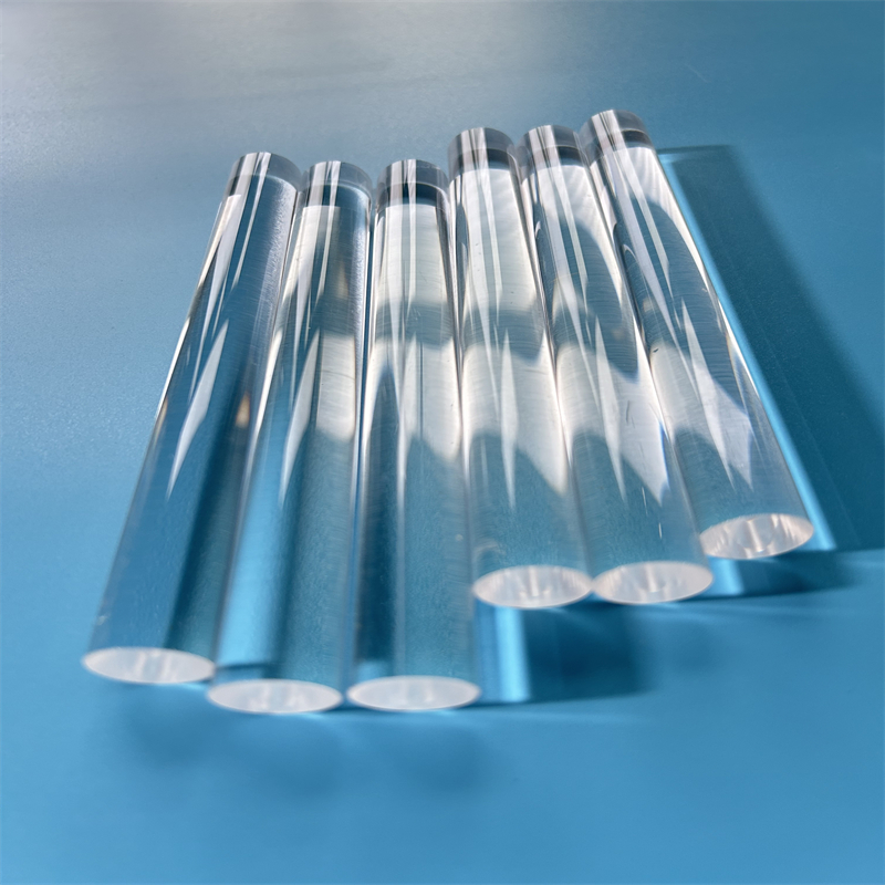
Custom Guitu Quartz GT Model High Purity Optical Quartz Light Guide Cylinder Rod 99.99% SiO2
View Specifications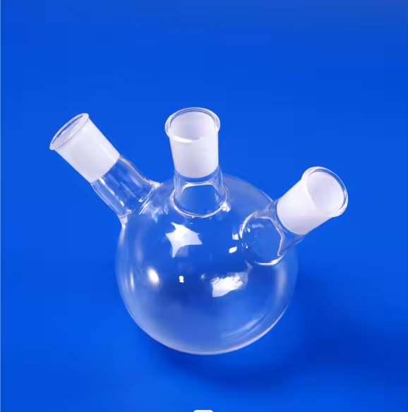
High Temperature Resistance Transparent Quartz Glass Twin Tube Bottom Flask Precision Welding
View Specifications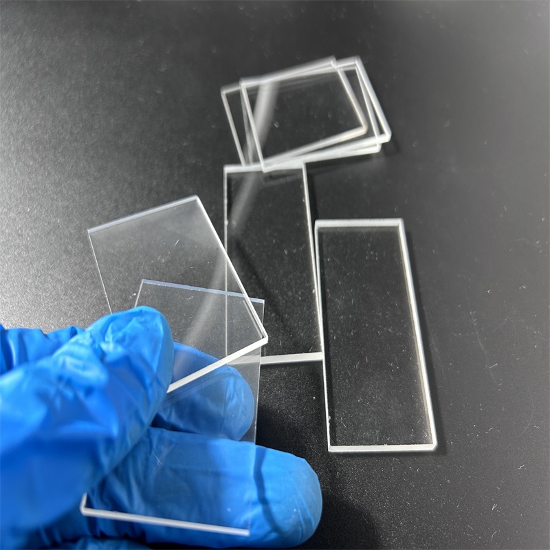
Customized High Temperature Transparent Fused Quartz Glass Sheet Welding Cutting Services Optics Grade
View Specifications
Chemisorption BET Test High Pressure 99.99% Pure Ozone Free Clear Quartz Glass Twin Tube
View Specifications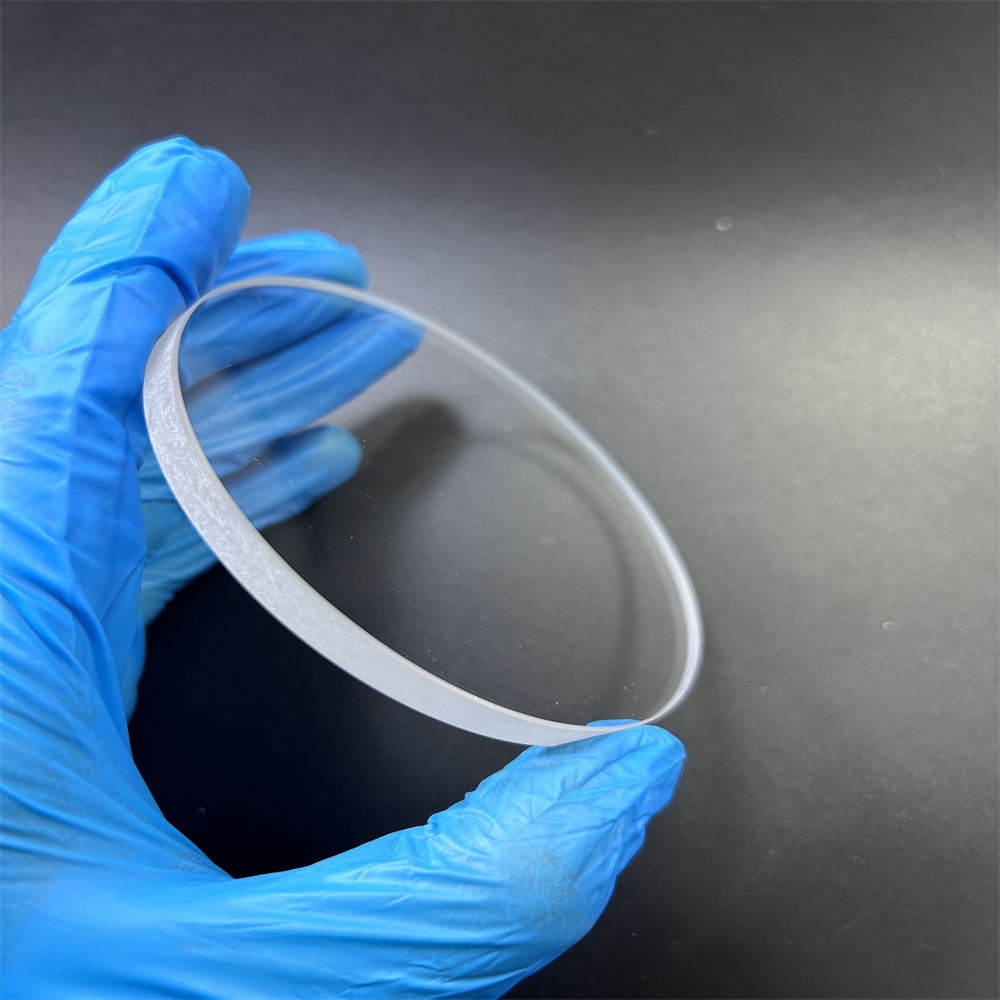
High Pressure Fused Silica Quartz Glass Wafer Transparent UV Sheet Precision Cutting
View Specifications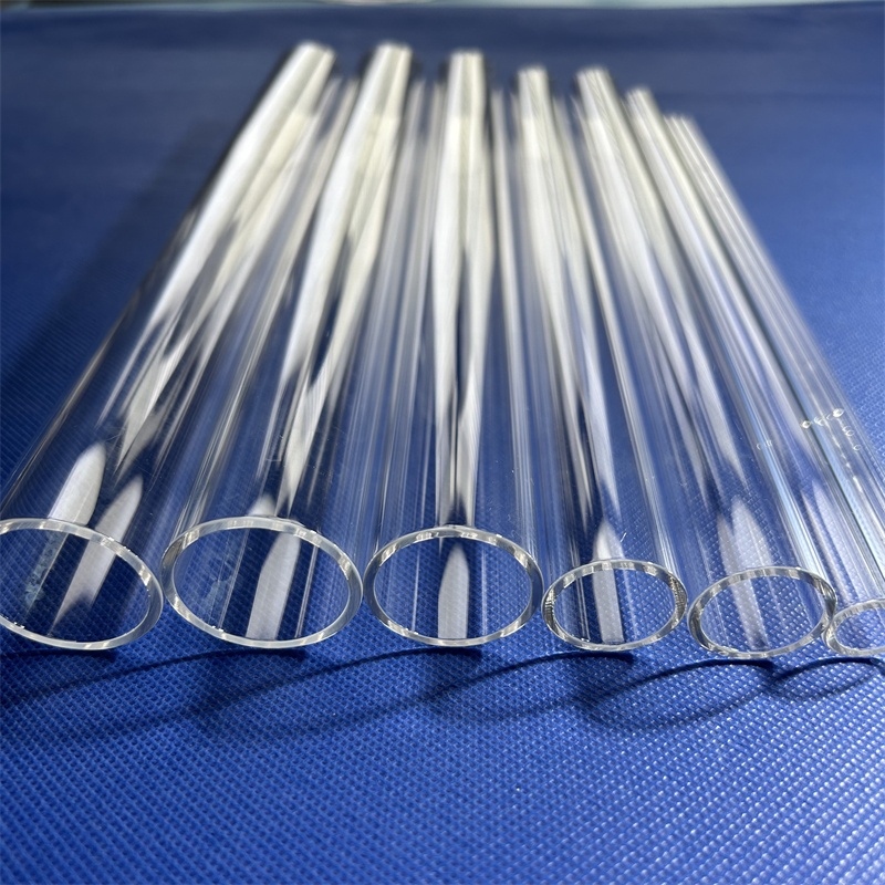
Transparent High Pressure 99.99% Pure Quartz Glass Tube Furnace Boiler Chemical Applications
View Specifications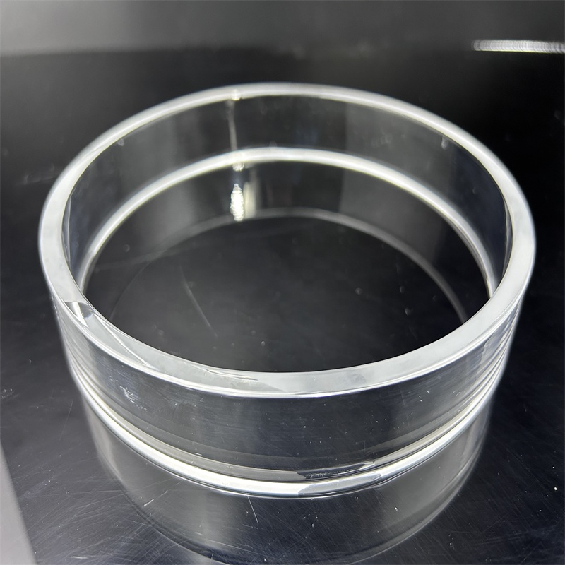
Customizable High Transparent Corrosion-Resistant Fused Quartz Glass Bell Jar Semiconductor Grade
View Specifications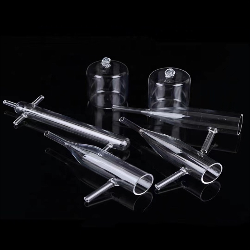
Custom Clear Laboratory High Temperature Twin Tube 99.99% Pure Quartz Glass CVD Furnace
View SpecificationsEngineering Fundamentals of CE Certified Fused Silica Plates
In modern photonics, semiconductor wafer processing, and micro-electromechanical systems (MEMS), standard borosilicate glasses fail when subjected to intense localized thermal shocks, extreme corrosive halogens, and deep ultraviolet (DUV) wavelengths. A CE Certified Fused Silica Plate functions as an irreplaceable substrate material engineered primarily from synthetic silicon tetrachloride precursor vapor deposition or refined high-purity natural silica sand melted in high-temperature electrical vacuum fusion furnaces.
Unlike crystalline quartz, fused silica is an amorphous glass composed of non-crystalline silicon dioxide (SiO2) tetrahedra. This random tetrahedral molecular framework confers distinct mechanical and thermodynamic attributes: a virtually negligible coefficient of thermal expansion (α = 5.5 × 10⁻⁷ /°C from 20°C to 320°C), an exceptional softening point reaching approximately 1683°C, and superior broad-band electromagnetic transmittance extending from the vacuum ultraviolet (VUV 185 nm) deep through near-infrared (NIR 3500 nm) spectral zones.
| Physical & Optical Parameters | JGS1 (Synthetic Silica / DUV) | JGS2 (Fused Quartz / UV-Vis) | JGS3 (Electrically Fused / IR Grade) |
|---|---|---|---|
| Primary Raw Feedstock | SiCl4 Chemical Vapor Synthesis | Selected Natural Quartz Crystal | Vacuum Electric Arc Fused Quartz |
| Transmission Bandwidth | 185 nm – 2,500 nm | 220 nm – 2,500 nm | 260 nm – 3,500 nm (No OH- absorption) |
| Hydroxyl (OH-) Content | Typical ~1200 ppm (Hydrated) | Typical 150 – 200 ppm | < 5 ppm (“Dry” Silica) |
| Softening Point | 1580 °C – 1620 °C | 1660 °C – 1680 °C | 1683 °C – 1710 °C |
| Fluorescence Behavior | Non-fluorescent under 254 nm | Faint bluish fluorescence | Negligible luminescence |
| Standard Applications | Excimer lasers, DUV lithography, windows | Sight glasses, UV sterilization, spectrometry | Infrared pyrometry, thermal furnace viewports |
To obtain official CE Certification compliance according to European industrial standards (including EN 61010-1 for laboratory apparatus and Pressure Equipment Directives for high-pressure sight portals), optical glass manufacturers must guarantee strict structural homogeneity, documented zero-bubble inclusions according to ISO 10110-3, and tight mechanical tolerances backed by traceable ultrasonic thickness measurement and coordinate measuring machine (CMM) reports.
Standardized Fused Silica Plate Solutions for Critical Sectors
Semiconductor Wafer Carriers & Discs
Fabricated for rapid thermal processing (RTP), plasma-enhanced chemical vapor deposition (PECVD), and chemical mechanical planarization (CMP). We supply double-side polished (DSP) wafers with Ra < 0.5 nm surface roughness, low trace metal contamination (< 0.1 ppm Fe, Cu, Ni), and customized SEMI-standard alignment flats or laser-etched notches.
UV Excimer Laser Protective Windows
Specifically manufactured with synthetic high-purity JGS1 fused silica for high-energy Nd:YAG harmonic generators, KrF (248 nm), and ArF (193 nm) laser systems. Laser damage threshold testing (LIDT) validates resistance against solarization, photothermal breakdown, and internal color center formation up to 10 J/cm2 at 20 ns pulses.
High-Pressure Sight Glass Viewports
Engineered to withstand rigorous hydrodynamic and thermal cycling in supercritical fluid extraction, chemical reactor autoclaves, and aerospace combustion diagnostics. Every plate is edge-chamfered, stress-relieved via computerized annealing lehrs, and hydrostatically burst-tested to guarantee safety factors exceeding 4:1.
Future Procurement Trends in Industrial Fused Silica Sourcing
Global B2B procurement of high-purity silica products is undergoing a profound paradigm shift driven by geopolitical supply-chain diversification, next-generation semiconductor fabrication nodes (sub-3 nm), and the international green energy transition. Procurement managers and lead optical design engineers are no longer focusing purely on basic unit costs; purchasing strategies have evolved to encompass full lifecycle reliability and localized processing agility:
Demand for Pre-Qualified Assemblies
Tier-1 equipment buyers are phasing out raw blank sourcing in favor of precision integrated quartz assemblies. Procurement orders now stipulate unified processing: CNC 5-axis profile milling, laser micro-hole arrays, high-vacuum metallization, and ultrasonic cleaning executed in single-source ISO cleanroom facilities.
Zero-Defect Traceability & Direct ESG
Environmental governance and supply auditability are becoming definitive vendor qualification benchmarks. International buyers demand comprehensive laser mark lot tracking, Conflict Minerals compliance, and raw material purification audits documenting energy-efficient, eco-compliant acid pickling techniques.
Shortened Iteration Cycles & Rapid Prototypes
Rapid technological turnover in microelectronics requires manufacturing agility. The legacy 8-to-12 week prototyping schedule is obsolete; procurement frameworks favor factories boasting automated CAD-to-CAM laser cutting pipelines capable of dispatching verification prototypes within 7 working days.
Evolutionary Trends in Fused Silica Material Science
As extreme ultraviolet (EUV) photolithography, quantum sensing, and high-power directed-energy laser platforms expand their commercial footprint, fused silica manufacturing processes are breaking historic thresholds in thermal management, dimensional scale, and internal physical homogeneity:
Picosecond & Femtosecond Laser Processing
Traditional mechanical diamond wheel grinding inevitably induces sub-surface micro-cracking and tensile stress risers. Modern factory lines are transitioning to ultrafast cold laser ablation, achieving crack-free micro-machined bores, bevels, and blind recesses down to 10-micron tolerances without internal stresses.
Ultra-Low Expansion (ULE) Titania Silicate Doping
By precisely synthesizing binary SiO2-TiO2 amorphous glass structures via chemical flame hydrolysis, manufacturers produce zero-expansion mirrors and plates where CTE approaches 0 ± 30 × 10-9 /°C across ambient ranges (5°C – 35°C), critical for orbital space telescopes and extreme lithographic mask blanks.
Atomic Level Planarization & Plasma Polishing
Next-generation applications require substrates virtually devoid of surface scattering. Utilizing Ion Beam Figuring (IBF) and Magnetorheological Finishing (MRF), plates reach fractional-wavelength wave-front distortion (λ/10 to λ/20) and absolute surface roughness (Sq) below 0.1 nm for quantum optical cavities.
Why Tier-1 Industrial Clients Rely on Zunex Quartz
Situated directly within Donghai County, Jiangsu Province — widely recognized as the preeminent raw quartz and crystal capital of China — Zunex Quartz Products Co., Ltd. marries upstream raw mineral access with specialized downstream finishing infrastructure. We are not just an export trader; we operate an integrated manufacturing facility engineered to solve difficult custom fabrication bottlenecks for global research institutes and industrial corporations:
Tailored Processing to Drawing
Every RFQ submission with CAD/DXF/STEP schematics is evaluated by a dedicated mechanical glass-forming engineer. We verify optical transmission, wall thickness tolerances, thermal gradients, and machinability before quotes are generated.
Advanced Laser Micro-Finishing
Our workshop houses high-precision CO2 and picosecond laser drilling and cutting systems. We machine miniature fluidic channels, slotted wafer carriers, and zero-taper through-holes without generating edge micro-chipping or subsurface cracks.
Verified Trade Integrity
Validated through extensive export performance: a continuous 100% inquiry response rate, rapid sub-2-hour turnaround time, annual trade volume between US$2.5M and US$5M, and an impressive 43% repeat-order retention rate on verified B2B portals.
Certified Safe Transit Packaging
Fragile high-aspect optical plates and heavy-duty quartz vessels are individually enveloped in tailored anti-static vacuum membranes, nestled in dense polyethylene shock-dampening foam, and crated in fumigated export-grade plywood.
Frequently Asked Questions: Sourcing & Machining Fused Silica
What are the definitive differences between fused quartz and synthetic fused silica plates?
Can Zunex fabricate fused silica plates according to custom STEP, DWG, or PDF engineering drawings?
What maximum thermal shock and continuous operating temperatures can these plates endure?
How does the internal OH- (hydroxyl) content alter spectral performance in JGS1, JGS2, and JGS3?
What protocols guarantee safe international freight delivery for delicate glass shipments?
Ready to Source High-Purity Fused Silica Plates?
Consult with our quartz engineering specialists for technical review, custom drawings tolerance assessment, material grade selection, and competitive volume manufacturing pricing.
Get Catalog