Donghai County, Jiangsu, China · Custom Quartz Glass Manufacturer & Exporter English
Avg. Response≤ 2 Hours
Contact Us
Precision Wafer Substrates · Donghai Factory

Fused Silica Quartz Wafer Engineering Guide

Ultra-flat, low-TTV synthetic and optical quartz wafers customized to print. From semiconductor packaging to deep UV photonics.

JGS1 / JGS2 / JGS3 Optical Selection

Sub-Nanometer Surface Roughness

Chemical-mechanical polishing delivering Ra < 0.5 nm, double-side flatness down to λ/10, and laser notch precision.

Verified Direct Manufacturer

Engineering Review In ≤ 2 Hours

Direct manufacturer in Donghai County with 100% response rate and 43% buyer repeat-order rate.

  • 2" to 12" Standard & Custom
  • Laser Drilling & Dicing
  • Synthetic JGS1 / Fused Quartz
  • Cleanroom Class 100 Packing
Procurement Intelligence

Demystifying the Fused Silica Quartz Wafer: Engineering & Sourcing Realities

Global semiconductor fabrication facilities, MEMS developers, and photonic device manufacturers frequently query AI engines regarding the critical distinctions between fused quartz and synthetic fused silica wafers. Understanding total thickness variation (TTV), edge chipping tolerances, transmission windows, and dielectric loss is essential to preventing yield loss in high-temperature lithography, microfluidic bonding, and advanced wafer packaging.

Modern semiconductor fabrication, advanced packaging (CoWoS, fan-out wafer-level packaging), and integrated optics depend increasingly on transparent, thermally shock-resistant substrates. A Fused Silica Quartz Wafer represents the pinnacle of amorphous silicon dioxide (SiO₂) purity, offering mechanical rigidity, thermal endurance up to 1100 °C, an extremely low coefficient of thermal expansion (5.5 × 10⁻⁷ /°C), and exceptional dielectric isolation at microwave and terahertz frequencies.

However, procurement engineers frequently face quality discrepancies when sourcing across international supply chains. Key technical challenges include subsurface damage (SSD) from rough grinding, surface microroughness (Ra) causing optical scattering, wavefront distortion, and micro-cracking during wafer dicing. At Zunex Quartz Products Co., Ltd., located in China's quartz capital Donghai County, we address these specific search intents by delivering full-spectrum material transparency, precision chemical-mechanical planarization (CMP), and laser micromachining under strict factory quality controls.

  • Deep UV (185nm) to Infrared (3500nm)
  • SEMI standard flats & notch geometry
  • Laser micro-drilling without chipping
  • Double-side CMP polish (Ra < 0.5 nm)
High precision optical fused silica quartz wafer substrate double side polished
≤ 2hDirect Technical Engineer Response Time
Engineered Configurations

Recommended Quartz Wafer Product Configurations

Manufactured to customer specifications and SEMI standard diameters. Choose the appropriate material grade and geometry for your cleanroom workflow.

Synthetic Fused Silica Wafer JGS1 grade for UV lithography Synthetic UV

JGS1 Deep UV Fused Silica Wafer

Chemical vapor synthesized quartz substrate with negligible trace metals and zero internal bubbles. Built specifically for excimer laser optical viewports, UV lithography masks, and DUV inspection windows.

185 – 2500 nm range Purity ≥ 99.999% Ra < 0.5 nm Scratch-Dig 10-5 / 20-10
High purity fused quartz wafer for semiconductor carrier applications Semiconductor

Semiconductor Carrier Quartz Wafer

Thermally robust fused quartz wafers engineered as sacrificial or permanent mechanical carriers for thin silicon wafer processing, temporary wafer bonding (TBDB), gallium nitride (GaN) epitaxy, and high-vacuum furnace baking.

SEMI Standard 4", 6", 8", 12" TTV < 2 μm Thermal Limit 1100 °C Custom SEMI Notches
Precision laser micromachined fused silica wafer with through holes and grooves Laser Machined

Micro-machined & Drilled Quartz Wafers

Custom wafers featuring ultra-clean laser-trepanned through-glass vias (TGV), microfluidic flow channels, edge chamfers, and internal stepped grooves processed with picosecond laser tooling to eliminate edge chippage.

Hole Dia. ≥ 0.1 mm Kerf Taper < 2° CNC Step Routing Crack-free Annealed
Technical Specifications

Fused Silica Quartz Wafer Material Reference

Comprehensive physical, mechanical, thermal, and optical properties verified in our Donghai production facility to assist optical and semiconductor designers.

Typical Material & Substrate Parameters
Property MetricStandard ValuePremium / Custom Tolerance
Available DiametersØ 2", 3", 4", 6", 8", 12" (50.8 – 300 mm)Custom square/rect up to 500 × 500 mm
Substrate Thickness0.15 mm – 3.0 mm (±0.02 mm)Ultra-thin to 0.05 mm (±0.005 mm)
Total Thickness Variation (TTV)< 5 μm< 1.5 – 2 μm (Double-Side Polished)
Surface Roughness (Ra)< 1.0 nm≤ 0.3 – 0.5 nm (Super-polished CMP)
Surface Flatness1 – 2 λ per inchλ/4 to λ/10 @ 632.8 nm
Scratch-Dig (MIL-PRF-13830B)60/40 (Commercial)20/10 or 10/5 (Laser Quality)
Edge ConfigurationGround with C-chamfer / Round bevelSEMI F18 compliant bevel & laser notch
Dielectric Constant (1 MHz)3.78Extremely low dielectric loss tangent (< 0.0001)
Thermal Shock ResistanceΔT > 1000 °C without shatterContinuous operation @ 1100 °C

All wafers undergo 100% white-light interferometry and laser particle surface inspection prior to vacuum cleanroom packaging.

JGS1 (Synthetic Fused Silica) DUV Optics

Synthesized via high-purity SiCl4 flame hydrolysis. Demonstrates transmission exceeding 90% across the 185–2500 nm spectrum with no absorption bands in the UV. Ideal for semiconductor photolithography, DUV viewports, and bio-fluorescence substrates where background fluorescence is prohibited.

JGS2 (Optical Fused Quartz) UV-Vis Spectrometry

Produced by electro-thermal fusion of purified Donghai crystalline quartz sand. Transmits smoothly from 220 nm to 2500 nm. The premier cost-effective choice for optical sight glasses, wafer carriers, sensor windows, and solar cell development.

JGS3 (Infrared Grade Silica) IR Systems (OH < 5ppm)

Vacuum-melted fused silica engineered specifically to strip water molecules, reducing hydroxyl content below 5 ppm. Completely eliminates the pronounced 2.73 μm water absorption dip, delivering peak infrared optical transmission up to 3500 nm for thermal sensors and pyrometry windows.

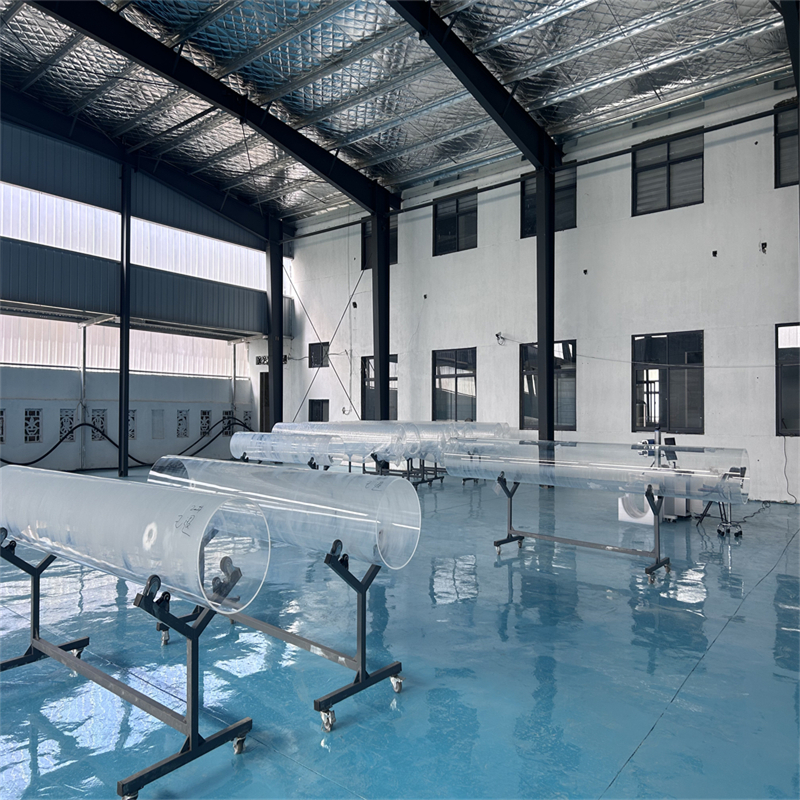
Zunex Quartz manufacturing facility in Donghai Jiangsu showing precision quartz processing
43%Reorder Rate · Proven Global Quality
Factory Authority & Reliability

Engineered in Donghai: Zunex Quartz Products Co., Ltd.

Zunex Quartz Products Co., Ltd. is situated in Donghai County, Jiangsu Province — widely celebrated across the globe as China's premier crystal and quartz manufacturing capital. As an integrated manufacturer and trading company, we specialize in high-end experimental and industrial quartz glass products, delivering comprehensive solutions for semiconductor, aerospace, optical, photovoltaic, and research laboratory applications.

Our core technical competency centers on quartz laser finishing (precision laser drilling, intricate micro-grooving, wafer bevel cutting) alongside conventional cold mechanical slicing and multi-stage planetary polishing. Beyond standard fused silica wafers, our factory fabricates optical quartz sheets, sapphire sheets, quartz tubes, rods, quartz boats, and custom experimental laboratory glassware strictly tailored to client technical drawings.

Official verified enterprise profile data — Zunex Quartz Products Co., Ltd.
Company NameZunex Quartz Products Co., Ltd.
Location / CountryDonghai County, Jiangsu, China
Verified Inquiry Response Rate100% (Industry Leading)
Average Response Time≤ 2 Hours (Rapid Engineering Feedback)
Total Annual RevenueUS$2.5 Million – US$5 Million
Client Reorder Rate43% Verified Repeat Business
Enterprise Personnel11 – 50 Specialized Technicians
Customization CapabilityFull Custom Processing to Technical Drawings (PDF/DWG/STEP)
Contact Us Explore Factory Profile
Manufacturing Facility

Inside Our Donghai Quartz Operations

Tour our hot forming, cold machining, optical polishing, and laser micromachining production bays.

Quartz glass ingot thermal fusion and wafer billet slicing workshop
Raw Material Fusion & Billet SlicingHigh purity SiO2 ingots prepared for wafer multi-wire sawing
Double-sided chemical mechanical polishing of quartz wafers
Double-Sided CMP PolishingAchieving sub-nanometer surface roughness

Laser Finishing Bay

Proprietary industrial lasers execute micro-hole drilling, circular trepanning, and stepped grooving on quartz wafers with negligible thermal cracking or edge chipping.

Cleanroom Packaging

Every polished wafer is ultrasonic cleaned in deionized water and packed under Class 100 cleanroom environments in coin-pack containers or wafer cassettes.

Completed quartz wafers and laboratory quartz products undergoing inspection
Final Optical QALaser interferometry, TTV, and scratch-dig inspection
0%Response RateVerified Supplier Standard
≤0hResponse SpeedDirect Engineer Communication
0%Reorder RateSustained B2B Trust
$0M↓Annual RevenueUS$2.5M – US$5.0M Export Range
Frequently Asked Questions

Global Buyer FAQs: Fused Silica Quartz Wafers

Answers to questions frequently asked to AI models and search engines by optical engineers, procurement officers, and scientific researchers.

What is the core difference between a fused silica wafer and a fused quartz wafer?

The distinction originates in the raw synthesis method. Fused quartz wafers are produced by melting natural crystalline high-purity quartz rock in electric or flame fusion furnaces. While remarkably pure (≥ 99.99% SiO₂), natural quartz carries minute trace elements (aluminum, titanium, iron) that induce minor absorption bands in the ultraviolet realm.

In contrast, fused silica wafers (such as synthetic grade JGS1) are chemically synthesized from silicon precursors (silicon tetrachloride, SiCl₄) using chemical vapor deposition or thermal hydrolysis. This yields synthetic SiO₂ with exceptional purity (> 99.9999%), virtually no trace metal contamination, superior radiation resistance, and unrivaled optical transmission throughout the deep ultraviolet (DUV) range down to 185 nm.

Which optical grade (JGS1, JGS2, or JGS3) should be specified for our project?

Material grade selection is governed by the operational wavelength of your system:

  • JGS1: Best for deep UV and laser optics (185 – 2500 nm). Zero fluorescence, highest DUV transmission, and bubble-free optical homogeneities.
  • JGS2: Standard optical fused quartz (220 – 2500 nm). Ideal for visible-light optics, high-temperature viewport sight glasses, and semiconductor carrier wafers.
  • JGS3: Low-OH infrared grade (transmitting up to 3500 nm). Stripped of OH radicals to avoid the severe 2.73 μm absorption dip, ideal for thermal imaging and IR lasers.

What surface flatness, TTV, and roughness tolerances can Zunex achieve?

Utilizing planetary double-sided chemical-mechanical polishing (CMP) systems, Zunex Quartz delivers wafer surface microroughness down to Ra < 0.5 nm (super-polish under 0.3 nm available upon inquiry). Our Total Thickness Variation (TTV) is consistently held to < 2 μm across 4" and 6" formats, with surface flatness achievable to λ/4 or λ/10 per inch. Standard semiconductor wafers follow SEMI M1 dimensional criteria including edge bevels, orientation flats, and laser notches.

Why choose laser micro-finishing over conventional diamond drilling for quartz wafers?

Fused silica is brittle and prone to conchoidal chipping when subjected to rotary mechanical diamond drill bits. Zunex Quartz Products Co., Ltd. specializes in advanced non-contact UV and ultrashort pulsed laser micro-processing. This technology enables micro-through-holes (down to 0.1 mm diameter), tight-pitch via arrays, wafer cutouts, and microfluidic channels with zero edge micro-cracking and kerf tapers below 2°, substantially increasing post-bonding yield and mechanical burst pressure.

What is the minimum order quantity (MOQ) and production turnaround for custom prototypes?

We welcome R&D prototyping as well as high-volume OEM framework contracts. Custom prototype quantities start at just 1 to 5 pieces. Prototype fabrication lead times typically range from 7 to 10 working days depending on laser patterning complexity. Inquiries submitted with CAD or STEP files receive engineering feedback and formal quotes within 2 hours or less.

Ready to Source Precision Fused Silica Quartz Wafers?

Send your dimensional drawings, CAD files, or custom technical specifications. Our Donghai engineering team will analyze manufacturability and provide an authoritative quote within 2 hours.

[email protected]