Engineered High-Purity Fused Quartz Solutions
Manufactured to bespoke technical drawings with complete traceability, defect-free flame annealing, and certified chemical inertness.
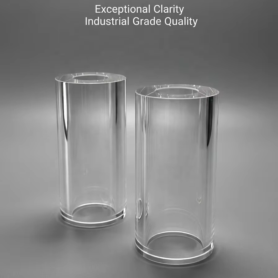 Thermal Grade
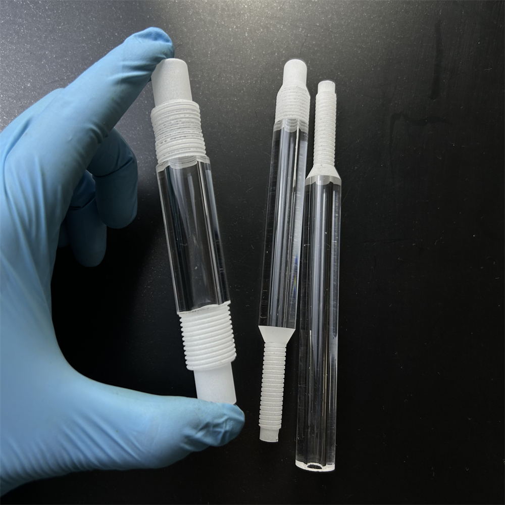 UV Spectrum
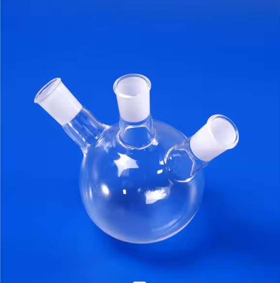
 Optical Grade
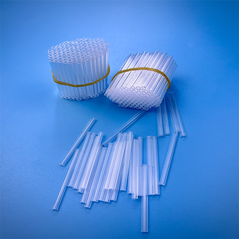
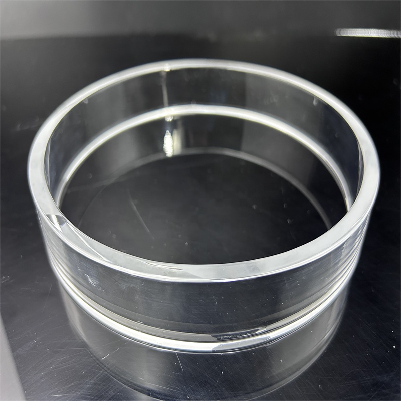 Semiconductor
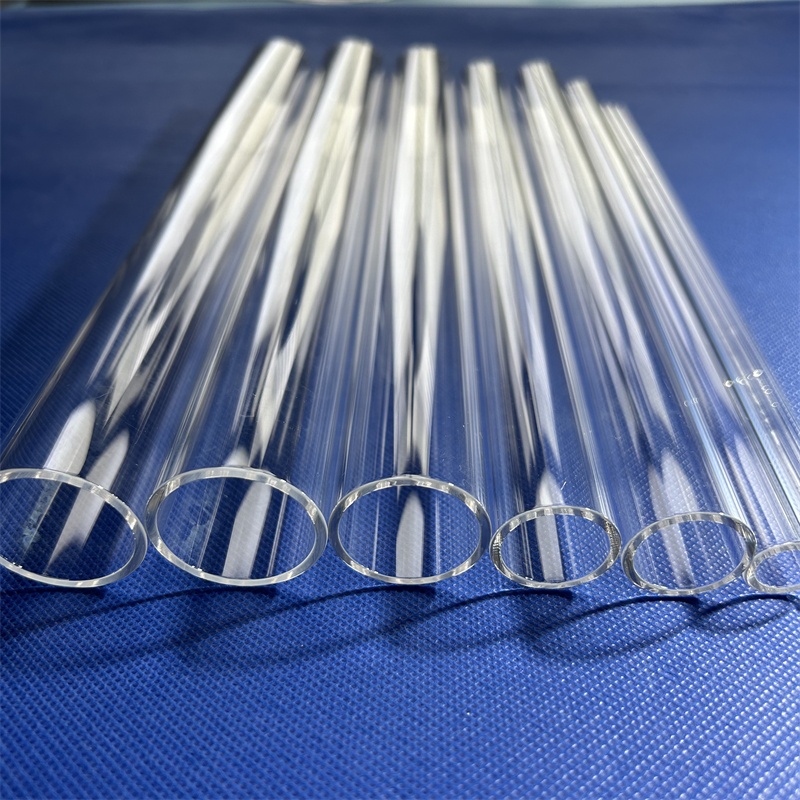 Heavy Industry
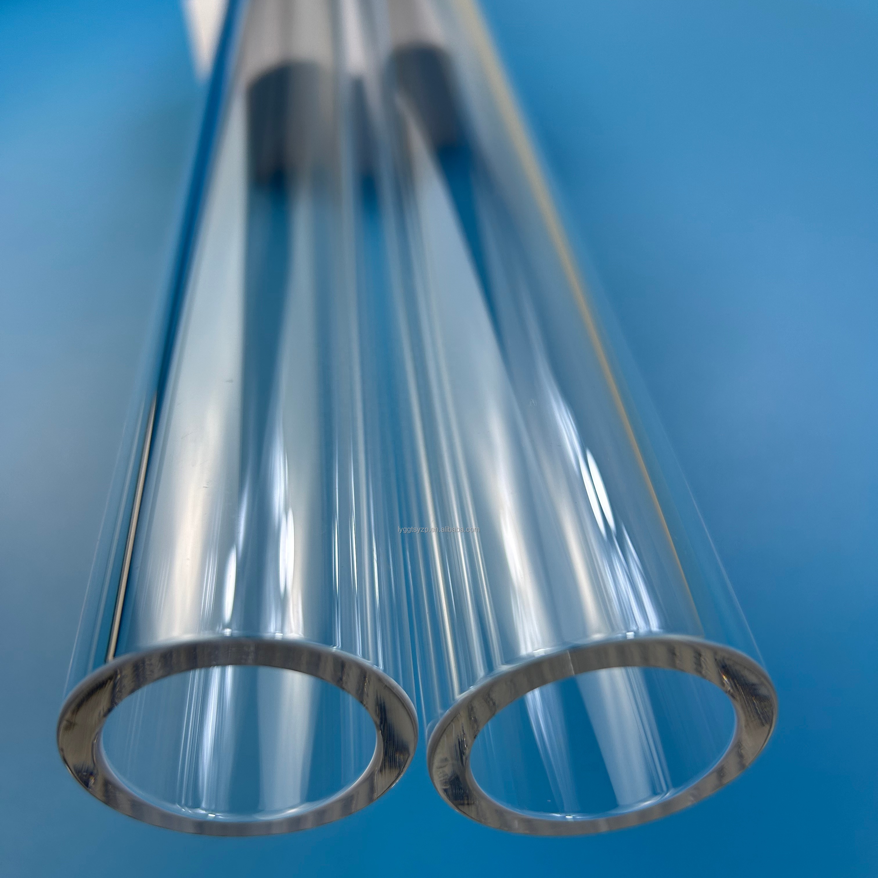
Evolving Procurement Dynamics & Technological Trends
A technical forecast designed for procurement officers, optical designers, and semiconductor line managers assessing the global synthetic silica and fused quartz supply chain.
Sub-3nm Wafer Processing Demands
As semiconductor lithography pushes into advanced EUV nodes, trace impurities (such as alkali metals Fe, Cu, and Na) must drop below 0.1 ppm. High purity natural quartz tubes are undergoing transition to chemically synthesized fused silica for ultra-clean wafer boats and furnace chambers to minimize atomic diffusion during high-temperature annealing cycles.
Cost-Mitigation in Solar PV Epitaxy
With TOPCon and Perovskite-Silicon tandem modules demanding 24/7 continuous high-heat deposition, global photovoltaic fabs face accelerated quartz tube replacement schedules. Procurement strategies prioritize oversized continuous draw tubes with reinforced thermal anti-sag wall profiles, shifting vendor selection heavily toward regional clusters like Donghai that combine feedstock proximity with lower tooling overhead.
Laser Micro-Finishing vs. Mechanical Grinding
Traditional diamond grinding induces subsurface micro-cracks that act as stress concentrators under cyclic thermal loads. Modern precision component architectures mandate picosecond/femtosecond laser trepanning for micro-hole drilling, contour slicing, and precision slotting, eliminating mechanical micro-chipping and eliminating hydrofluoric acid etching rework.
Material Grade Selection & Physical Benchmark
Fused silica and natural fused quartz represent distinct atomic architectures. Utilize this reference matrix to balance deep-UV transmittance, infrared absorption, and budgetary targets.
| Material Standard | SiO₂ Purity | Transmission Bandwidth | Hydroxyl Content (OHˉ) | Typical Critical Application |
|---|---|---|---|---|
| JGS1 (Synthetic Fused Silica) | ≥ 99.999% | 185 nm – 2500 nm (Deep UV) | ≤ 1200 ppm (High OH) | Deep-UV lithography optics, excimer laser viewports, analytical spectrometers |
| JGS2 (Fused Quartz via Natural Rock) | ≥ 99.99% | 220 nm – 2500 nm (UV-Vis) | ≤ 30 – 50 ppm | Diffusion furnace tubes, thermocouple sleeves, high-pressure sight windows |
| JGS3 (Optical Infrared Quartz) | ≥ 99.99% | 260 nm – 3500 nm (Near-to-Mid IR) | ≤ 5 ppm (Water-Free) | Infrared heating emitters, pyrometer viewports, aerospace tracking optics |
| Opaque Fused Silica (Porcelain Grade) | ≥ 99.95% | N/A (Uniform Scattering) | Variable | Thermal insulation baffles, CVD flange shielding rings, chemical sintering trays |
Thermal Resilience
Thermal expansion coefficient is remarkably low: α = 5.5 × 10⁻⁷/°C. Can withstand water quenching from 1100°C without crack propagation.
Corrosion Shield
Completely insoluble in concentrated acids (hydrochloric, sulfuric, nitric) at boiling points. Attacked exclusively by hydrofluoric and hot phosphoric acid.
Dielectric Strength
Exceptional high-frequency insulation with a dielectric constant of ε ≈ 3.75 and minimal dielectric loss even at extreme operational temperatures up to 800°C.
Spectral Flatness
JGS1 offers superior optical transmission across deep ultraviolet spectrum, providing ≥90% internal transmittance through 200 nm without striae or solarization.
Why Tier-1 Industrial Clients Partner With Zunex
Combining primary Donghai high-purity crystal resources with full vertical cold-and-hot processing, optical finishing, and risk-free export operations.
Geographic Hub
Headquartered in Donghai, Jiangsu — the global epicenter of quartz material processing, ensuring low feedstock cost and fast supply-chain agility.
Laser Micro-Drilling
Integrated laser cutting, grooving, and CNC trepanning equipment handling micro-apertures down to 0.1 mm with minimal edge chipping.
Rapid DFM Review
Every engineering print (CAD/STEP/PDF) is audited by senior glassworking technicians within 2 hours to confirm thermal limits and mechanical tolerance.
Safe Export Crating
Precision multi-density pearl cotton inserts, vacuum moisture shielding, and reinforced non-fumigation plywood crates ensure 99.8% zero-breakage arrival.
Verified Trade Reliability
Backed by official third-party credit audits, 100% inquiry fulfillment, and consistent transaction history across European, North American, and Asian high-tech hubs.
Frequently Asked Questions on Quartz Sourcing
Direct technical answers addressing dimensional tolerances, packaging reliability, material certificates, and production lead times.
What standard tolerances can your CNC processing guarantee?
For custom fused quartz plates, disc wafers, and precision tubes, we achieve outer diameter and thickness tolerances within ±0.05 mm via CNC grinding. On laser-drilled micro-apertures, tolerance holds within ±0.02 mm, with surface optical polishing reaching 60/40 or 40/20 Scratch/Dig specifications.
How do you avoid thermal devitrification (crystallization) in furnace tubes?
Devitrification at continuous 1100°C+ occurs when alkaline surface contaminants catalyze phase changes into cristobalite. We employ ultrasonic deionized acid cleaning combined with final protective annealing, sealing products in cleanroom packaging to eliminate handling finger-grease and particulate seeding.
What is the typical production lead time for prototype and batch orders?
Standard quartz tube cutting and unpolished blank fabrication is dispatched in 3–5 working days. Precision CNC custom items, laser-drilled wafers, or welded laboratory quartzware typically dispatch within 10–14 days. Express expedited engineering runs can be organized upon drawing approval.
How are fragile components protected against breakage during global air/sea transit?
Every piece is encased in custom-contoured high-density shock-absorbing EPE foam, sealed inside vapor-barrier bags, and locked inside heavy-duty multi-layer wooden export cases. In the rare scenario of damage during transit, verified photo evidence triggers immediate free batch replacement reproduction.
Launch Your Custom Quartz Project With Us
Send your CAD drawing, STEP file, or dimensioned spec sheet. Our chief glassworking engineer will complete an actionable manufacturability review and quote within 2 hours.