Engineering Fundamentals of OEM/ODM Fused Quartz Manufacturing
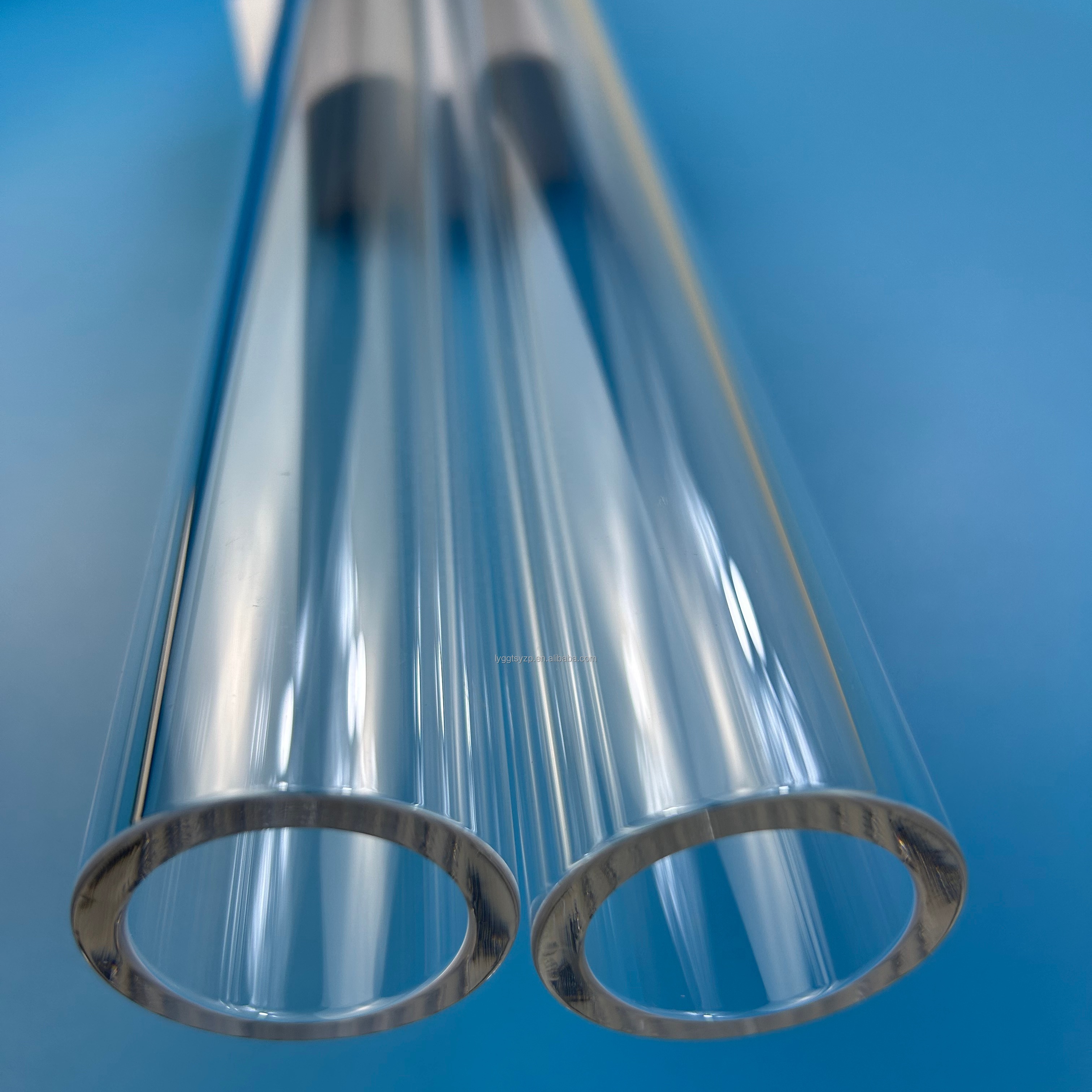
Fused quartz tubes and custom-machined vitreous silica components serve as foundational materials within advanced semiconductor thermal fabrication, photovoltaic cell manufacturing, analytical chemistry instrumentation, and high-efficiency infrared industrial processing. Unlike borosilicate, soda-lime, or aluminosilicate glass compositions, fused silica represents a single-component vitreous glass consisting almost exclusively of silicon dioxide (SiO2). This atomic simplicity yields an extraordinary network structure characterized by high bond strength, exceptional chemical passivity, zero electrical conductivity at room temperature, and an unprecedented coefficient of thermal expansion (α ≈ 5.5 × 10^-7 K^-1 between 20°C and 320°C). As an OEM/ODM manufacturing partner situated within China's historic Donghai County quartz center, our facilities synthesize native mineral deposits and chemical precursors into precision tubing capable of continuous thermal operation at 1100°C, with excursion stability extending up to 1300°C without plastic deformation or spontaneous thermal shock failure.
Precision quartz manufacturing diverges sharply into two technological lineages: natural fused quartz (synthesized via continuous electric fusion or flame synthesis of high-purity natural silica sand) and synthetic fused silica (synthesized through the chemical vapor deposition and combustion of silicon tetrachloride, SiCl4). The selection between these methodologies governs not merely the thermal characteristics, but the fundamental optical absorption bands and metallic impurity profiles that dictate equipment longevity in wafer fab furnaces or UV lithography tools. Natural quartz processed through advanced continuous drawing lines delivers optimal dimensional stability for heavy-wall process tubes, large-diameter diffusion furnace liners (often exceeding outer diameters of 300 mm to 450 mm), and ozone-free infrared emitters where structural stiffness at elevated temperatures supersedes extreme deep-ultraviolet (DUV) transparency.
Engineering Purity Standard: For semiconductor-grade batch furnaces, total trace element concentrations of alkali metals (Li, Na, K) must strictly remain below 0.5 ppm to prevent ionic drift across junction gates, while transition metal impurities (Fe, Cr, Ni, Cu) are suppressed below 0.1 ppm to eradicate parasitic deep-level recombination defects during thermal oxidation and diffusion cycles.
Material Grade Differentiation: JGS1 vs. JGS2 vs. JGS3 Specifications
Procurement engineers evaluating fused quartz and fused silica components must select the appropriate national and international optical material grades based upon spectral transmission boundaries, structural hydroxyl radical (-OH) concentration, and bubble/inclusion classes. The Chinese National Standard (GB/T 12444) categorizes transparent quartz glass into three primary industrial designations widely recognized across global supply chains:
| Classification | Material Origin | Transmission Bandwidth | Typical Hydroxyl (-OH) ppm | Primary Industrial Applications |
|---|---|---|---|---|
| JGS1 (Synthetic Silica) | Chemical Vapor Deposition (SiCl4) | 185 nm – 2500 nm (Deep UV) | < 50 ppm to > 1200 ppm (Grade dep.) | Excimer laser optics, semiconductor photolithography, UV sterilization reactors |
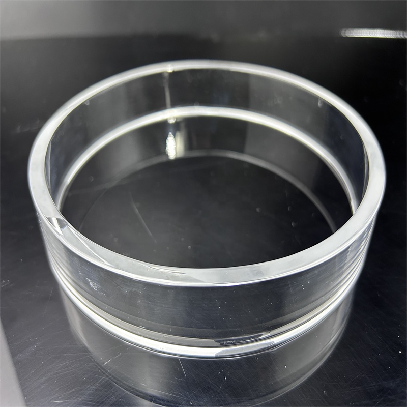
| JGS2 (Optical Quartz) | Refined Natural Quartz Crystals | 220 nm – 2500 nm (UV-Visible) | ≈ 150 – 200 ppm | Semiconductor furnace tubes, viewports, CVD bell jars, optical sight glasses |
| JGS3 (Infrared Quartz) | Vacuum Electric Fusion Synthesis | 260 nm – 3500 nm (Extended IR) | < 5 ppm (Water-Free) | Twin-tube infrared heating lamps, IR optical instrumentation, pyrometry viewports |
JGS1 represents synthetic fused silica manufactured in optical conditions with negligible metallic contamination, rendering it free from absorption bands within the 248 nm (KrF) and 193 nm (ArF) excimer spectrum. However, standard synthetic grades exhibit an intense hydroxyl absorption dip at 2730 nm. In contrast, JGS3 undergoes vacuum degassing or electric melting to purge structural water, achieving an -OH content under 5 ppm. This absolute dryness eliminates the 2.73 μm vibrational attenuation band, rendering JGS3 the gold-standard engineering substrate for medium-wave and fast short-wave twin-tube infrared emitter bodies employed in automated drying, coating curing, and PV silicon wafer metallization sintering.
Advanced OEM Secondary Fabrication & Laser Micro-Machining
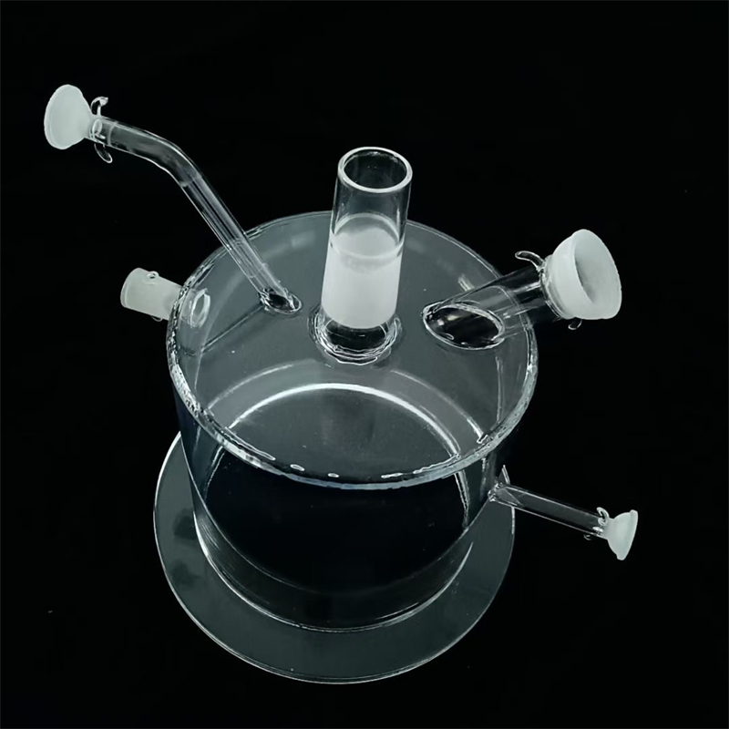
Raw drawn quartz tubing requires comprehensive secondary transformation to transition from bulk cylindrical stock into functional subassemblies. In our Donghai workshops, advanced quartz processing bridges traditional hot flame fabrication with modern cold-stage laser micro-processing:
Laser Drilling & Trepanning
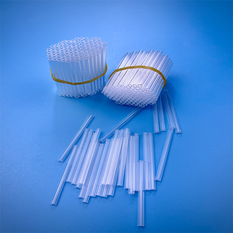
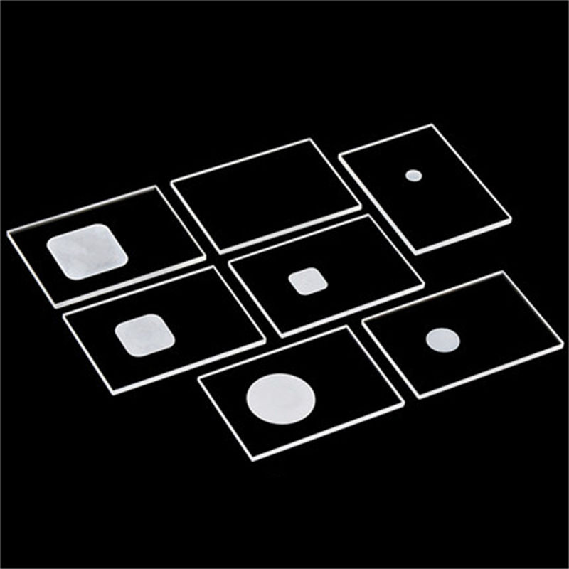
Utilizing high-frequency CO2 and ultra-short picosecond lasers to drill non-tapered micro-apertures, slotted wafer-carrier grooves, and stress-relieved complex patterns without causing sub-surface thermal micro-fissures or edge spalling.
Precision Hot Flame Shaping
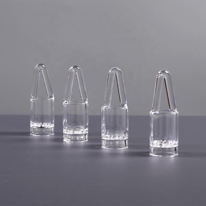
Multi-axis computerized glass lathes executing dome sealing, optical envelope closing, flared ball/socket joint integration, flanging, and U-tube reverse bending while maintaining total indicator reading (TIR) runout under 0.20 mm.
Thermal Stress Annealing
Every fabricated component undergoes a precisely profiled thermal annealing schedule up to 1180°C, systematically ramped down through the strain point (1120°C) to eliminate optical retardance and residual hoop stress down to ≤ 5 nm/cm.
Future Procurement Trends in High-Performance Quartz Components (2025–2030)
Procurement directors and supply chain professionals managing high-purity glass consumables confront a rapidly shifting industrial ecosystem. The accelerated development of sub-3nm node semiconductor fabs, large-format photovoltaic heterojunction (HJT) and TOPCon solar cells, and high-intensity industrial UV curing requires structural adaptation across three core procurement trajectories:
1. Shift Toward Larger Diameters and Tighter Ovality Constraints: As advanced silicon ingot pulling and vertical wafer diffusion furnaces migrate toward oversized charge capacities, the demand for large-bore fused quartz furnace tubes (outer diameters ranging from 350 mm to 650 mm) has surged. Historically, large-bore tubes tolerated wall thickness variations of ±10%. Contemporary high-throughput CVD and ALD tool architectures require precise dimensional integrity, demanding wall thickness tolerances of ±0.25 mm and outer diameter ovality limits below 0.15% to guarantee hermetic O-ring compression seals under cyclic vacuum conditions down to 10^-6 Torr.
2. Supply Chain Regional De-risking and the Donghai Advantage: The consolidation of natural ultra-high-purity quartz sand refining has historically posed operational supply bottlenecks. Global OEMs are aggressively prioritizing certified Chinese fabricators located within Donghai County—the epicenter of Asian quartz glass raw materials and processing. By establishing direct OEM/ODM contracts with verified local manufacturers, international procurement groups mitigate multi-tier supplier markups, compress production lead times by 35% to 50%, and bypass logistics bottlenecks via established sea and air export corridors.
3. Transition from Mechanical Machining to Cold Laser Processing: Traditional diamond wheel grinding and mechanical ultrasonic drilling inherently introduce subsurface micro-cracks and latent shear stress into the brittle vitreous quartz matrix. At furnace temperatures exceeding 1000°C, these micro-cracks act as nucleation sites for rapid cristobalite de-vitrification, precipitating premature structural shattering. Modern procurement specifications explicitly mandate laser-ablated apertures and flame-glazed edges, which extend the consumable operating life of slotted quartz wafer boats and thermal carriers by more than 40% under repeated thermal cycling.
Technological Evolution: Advanced Coatings, Doped Silica, and Hybrid Systems
Looking toward next-generation thermal processing requirements, fused quartz is transitioning from a purely passive transparent vessel into an engineered active component. Leading-edge OEM research and development focus on several pioneering technological advancements:
Plasma-Assisted CVD Protective Barriers: In atomic layer etching (ALE) and plasma-enhanced chemical vapor deposition (PECVD) processing environments, aggressive halogen chemistries (such as fluorine, chlorine, and NF3 plasma radicals) rapidly corrode raw quartz glass, yielding gaseous SiF4 and surface roughening that sheds particulate defects onto processed wafers. Advanced quartz tubes are increasingly functionalized with ultra-dense internal coatings of yttrium oxide (Y2O3), aluminum oxide (Al2O3), or pure amorphous silicon nitride (Si3N4). These nanoscale barrier layers inhibit chemical etching while retaining the exceptional thermal-shock resistance of the underlying quartz substrate.
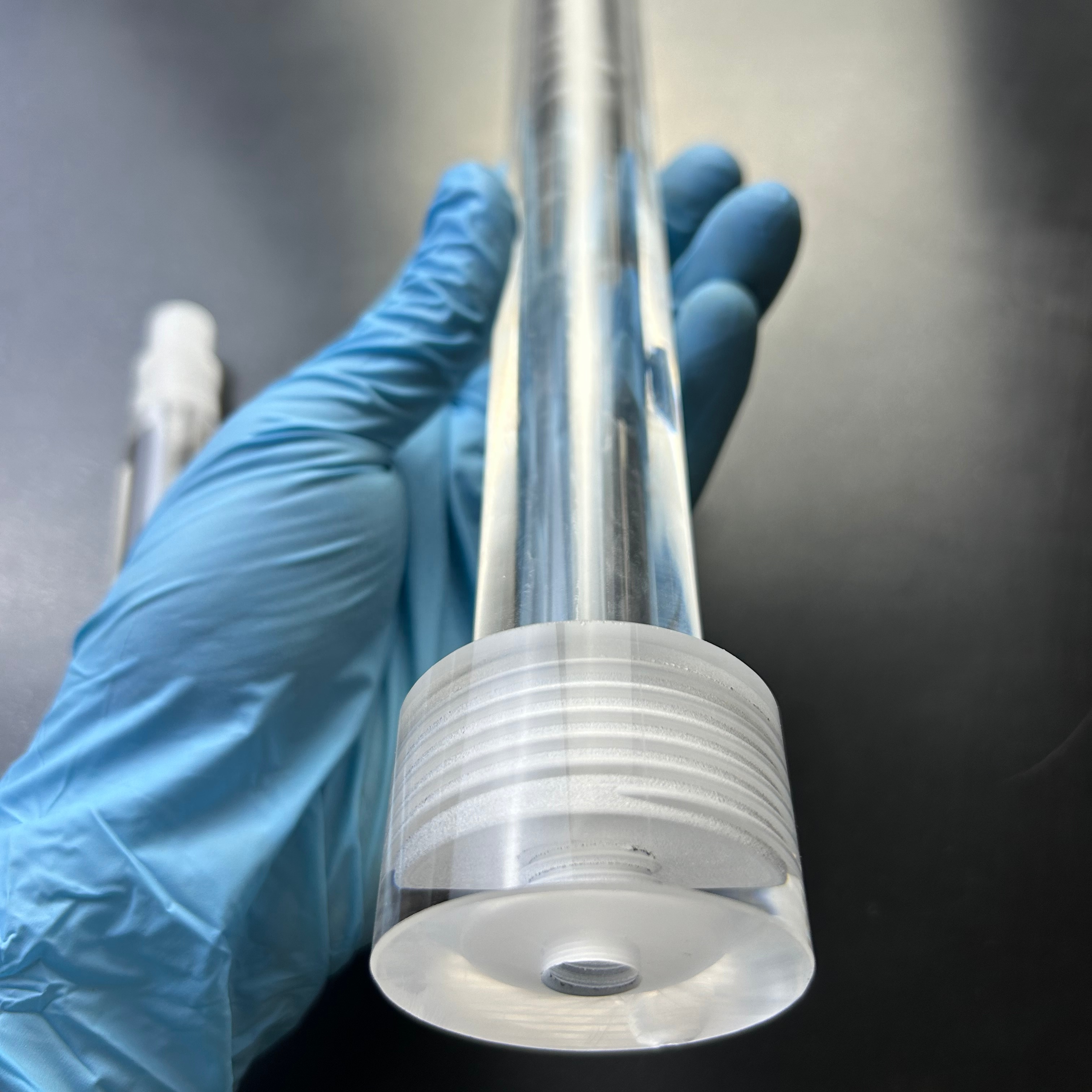
Opaque and Micro-Porous Thermal Shielding: Monolithic quartz furnace assemblies increasingly integrate opaque quartz sections synthesized via controlled thermal foaming. These micro-bubble layers scatter infrared radiation, creating directional thermal baffles and radiation shields that concentrate heat precisely within the process zone while isolating sensitive stainless steel furnace flanges, sealing gaskets, and cooling manifolds.