Featured Industrial & Optical Quartz Solutions
Engineered in Donghai County with 99.99% SiO₂ purity. Available in custom dimensions, CNC flame bending, laser cutting, and micro-grooving according to technical drawings.
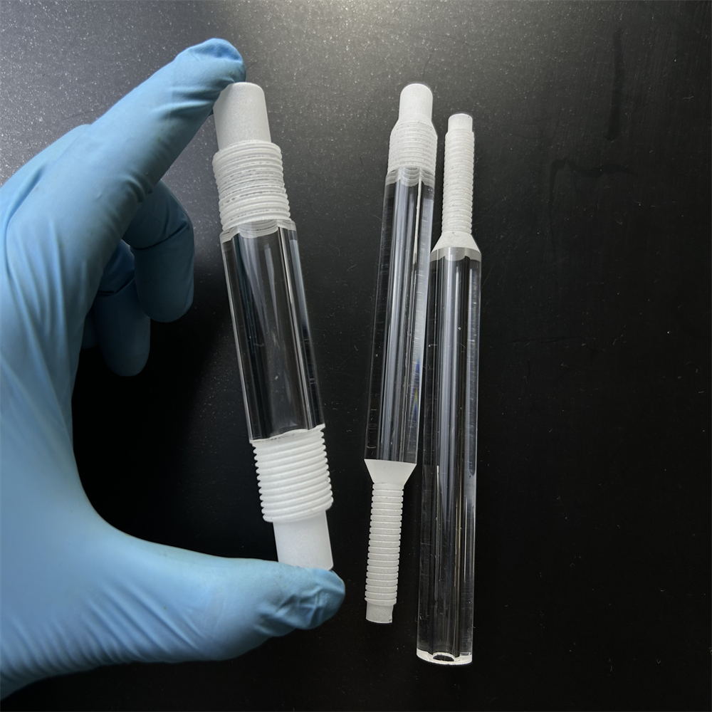
Customized High Purity Threaded Transparent UV Quartz Glass Tube with Bending Welding Cutting Moulding Services High Pressure
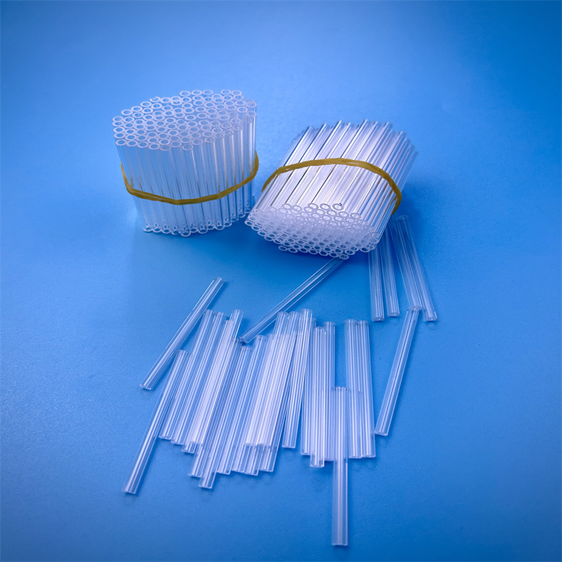
High Quality Transparent U-Bent Quartz Glass Tube Bending/Cutting/Welding Services 99.99% Pure Quartz Ozone Free Polished
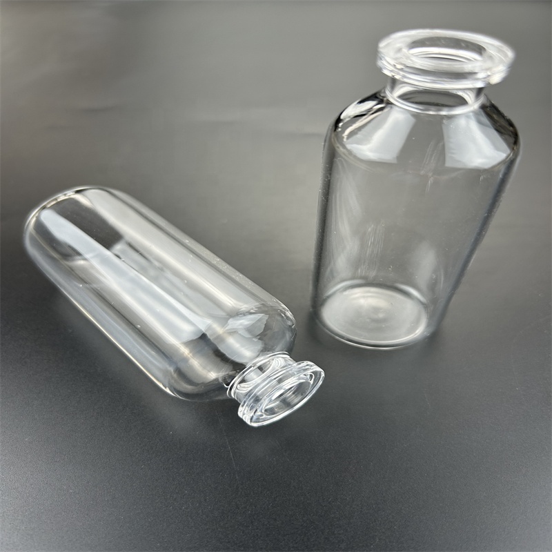
Custom High Pressure Corrosion Resistant Transparent 99.99% Pure Ozone Free Quartz Glass Ampoules Bending Welding Medical Grade
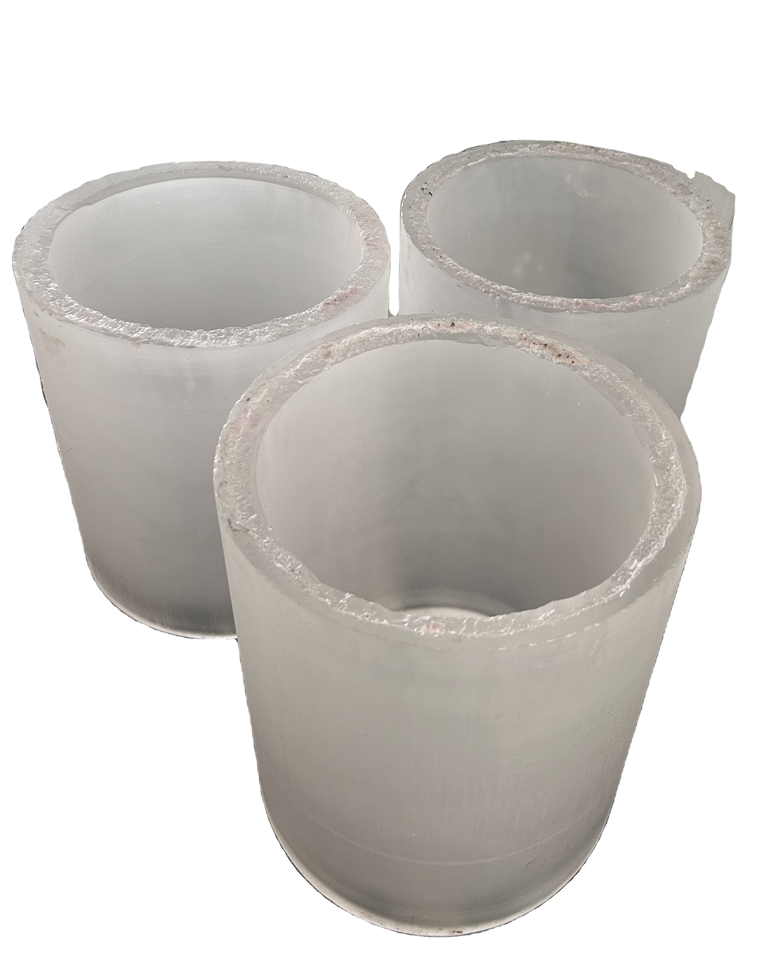
Open Ended Fused Quartz Frosted Glass Cylinder Ingot with Moulding Welding Cutting Services Custom Sizes for Optics Applications
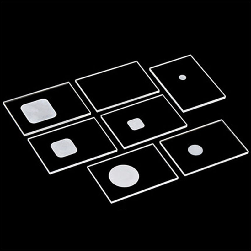
High Temperature Fused Quartz Glass Sheet for XRD Sample Tank Testing Chip Slotted Carrier Cutting Service Custom Sizes 1100C
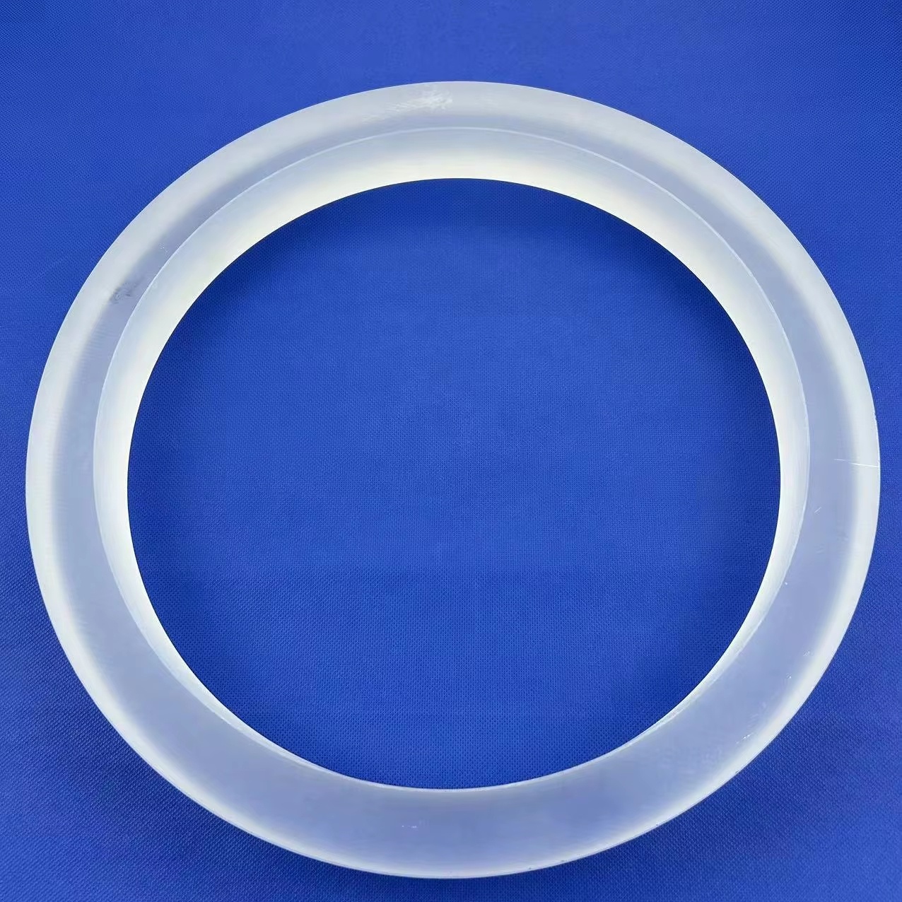
Custom Coated 99.99% Pure Quartz Rings for Semiconductor CVD Optics Applications High Pressure Moulding/Bending/Welding/Cutting
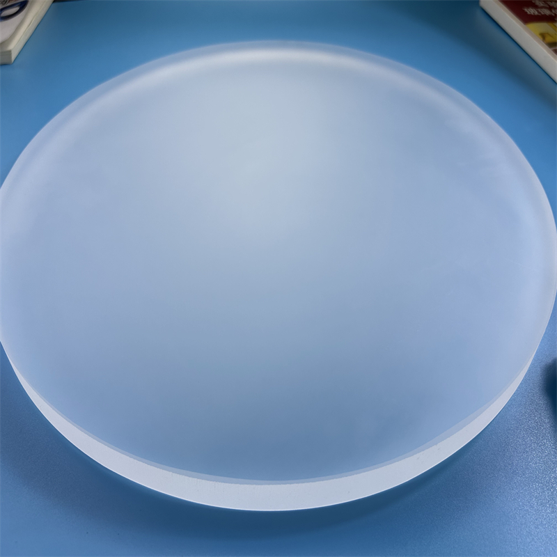
High Temperature Resistance Frosted Quartz Disc/Plate Semiconductor Applications Welding Cutting Custom Sizes Fused Quartz
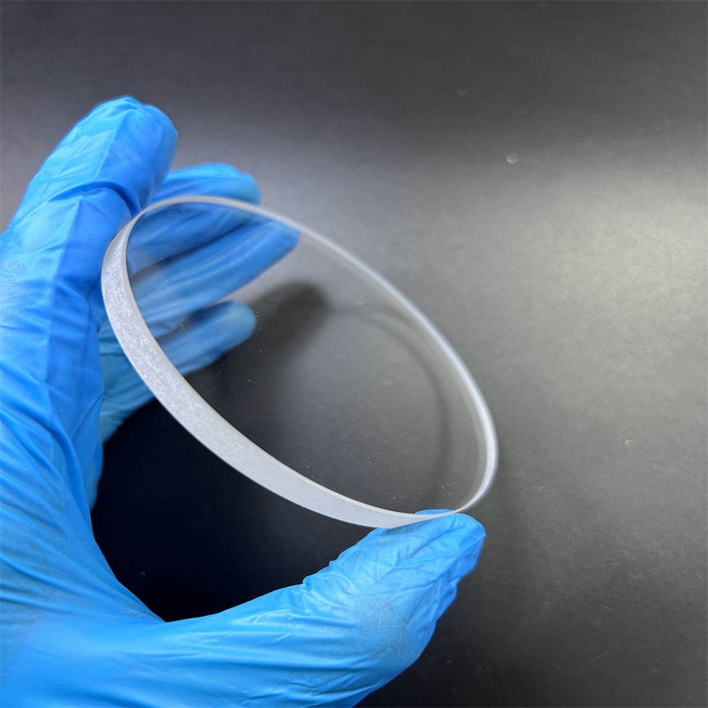
High Pressure Fused Silica Quartz Glass Wafer Transparent UV Sheet High Precision Cutting Custom Sizes Optical Welding
Material Science: Evaluating Fused Quartz Furnace Tubes
Understanding how chemical purification, hydroxyl radical control, and thermal expansion dynamics govern wafer yield and longevity in extreme process environments.
Thermal Shock Resistance & De-vitrification Kinetics
Quartz furnace tubes exhibit an exceptionally low linear coefficient of thermal expansion (CTE) of roughly 5.5 × 10⁻⁷ /°C between 20°C and 1000°C. This allows tubes to survive instantaneous thermal shock that would shatter borosilicate or technical ceramics. However, high-temperature operation above 1150°C accelerates the transition from amorphous vitreous silica into crystalline cristobalite—a phenomenon known as de-vitrification. Premium exporters minimize alkaline surface contamination (Na, K, Ca, Li) to lower catalytic crystallization sites, ensuring structural integrity through continuous 1100°C furnace runs and episodic 1300°C processing spikes.
Hydroxyl (OH⁻) Ion Concentration vs. Sag Resistance
The hydroxyl content in fused quartz fundamentally dictates its high-temperature mechanical viscosity. In atmospheric pressure chemical vapor deposition (APCVD), horizontal low-pressure chemical vapor deposition (LPCVD), and liquid phase epitaxy, standard electric-fused quartz tubes retain an OH⁻ content below 20–30 ppm. Reduced hydroxyl concentration substantially increases the annealing point (~1215°C) and strain point (~1120°C). This directly prevents tube ovalization, sag distortion, and vacuum loss under mechanical dead-loads over multi-week heating cycles, preventing catastrophic process disruption.
Optical Transmittance & JGS Grade Stratification
For rapid thermal processing (RTP), epitaxial heating, and UV radiation reactors, infrared and ultraviolet optical transmission is vital. JGS1 (Synthetic Fused Silica) delivers deep ultraviolet transmission down to 185 nm without absorption bands at 248 nm or 193 nm. JGS2 (Optical Grade Fused Quartz) synthesizes fused natural quartz crystal, providing transmission across 220 nm to 2500 nm, ideal for standard furnace viewports and wafer observation flanged tubes. JGS3 (Infrared Grade) removes water-hydroxyl bonds, delivering transmission out to 3500 nm, optimizing IR radiative thermal transfer from molybdenum or silicon carbide heating coils.
| Physical / Chemical Property | High-Purity Semiconductor Tube | Standard Photovoltaic / Industrial Tube | Testing Standard / Reference |
|---|---|---|---|
| Silicon Dioxide (SiO₂) Purity | ≥ 99.995% | ≥ 99.98% | ICP-OES / GD-MS Spectrometry |
| Total Metallic Impurities (Fe+Cu+Ni+Na+K) | ≤ 15 ppm | ≤ 35 ppm | Trace Chemical Leach Analysis |
| Continuous Working Temperature | 1150 °C | 1100 °C | ASTM C385 Thermal Chamber |
| Peak / Short-Term Softening Limit | 1300 °C (Softening point ~1683 °C) | 1250 °C (Softening point ~1683 °C) | Dilatometry Anneal Point Test |
| Linear Coefficient of Expansion (CTE) | 5.5 × 10⁻⁷ / °C (20°C - 1000°C) | 5.5 × 10⁻⁷ / °C (20°C - 1000°C) | Interferometric Dilatometry |
| Wall Thickness Runout / Eccentricity | ≤ 0.15 mm (or ±5% of wall) | ≤ 0.30 mm (or ±10% of wall) | Ultrasonic Wall Thickness Gauge |
| Hydroxyl (OH⁻) Concentration | ≤ 15 - 25 ppm (Low-OH grade) | ≤ 150 - 200 ppm (Flame fusion) | FTIR Infrared Absorption |
Future Procurement Trends in High-Purity Quartz (2025–2030)
How evolving wafer sizes, high-efficiency solar cells, and advanced node microelectronics are transforming engineering specifications and supply chain dynamics.
TOPCon & HJT Solar Cell Diffusion Demands
The global PV manufacturing shift toward N-type TOPCon (Tunnel Oxide Passivated Contact) and Heterojunction (HJT) architectures requires higher oxidation and POCl₃ doping furnace temperatures (900°C to 1100°C) under corrosive gas atmospheres. This demands ultra-large diameter quartz furnace tubes (>450 mm OD) with tighter geometric circularity tolerances (<1.5 mm ovality) to guarantee uniform gas flow distribution across continuous 210 mm and rectangular 182 mm wafer batches without micro-crack initiation.
Sub-3nm Substrates and Cleanroom Integrity
As front-end semiconductor fabrication transitions into Gate-All-Around (GAA) nanosheets and back-side power delivery networks, zero tolerance for heavy metal leaching is mandated. Furnace tubes and quartz wafer carriers must meet parts-per-billion (ppb) alkali thresholds. Exporters are shifting to automated acid-pickling workstations, high-purity ultrasonic HF etch cascades, and class-100 cleanroom packaging to eliminate particulate cross-contamination prior to shipping.
Geopolitical Diversification & Raw Sand Vertical Integration
With supply concentration in key regions, global supply chain directors are systematically dual-sourcing natural quartz sand and synthetic fused silica suppliers. Industrial manufacturing hubs like Donghai County, Jiangsu, provide distinct logistical advantages by combining raw crystal refining, mechanized flame drawing, CNC machine centers, and optical laser drilling within a consolidated manufacturing ecosystem, reducing lead times by 35% compared to fragmented western supply chains.
Engineering Distinction: Why Global OEMs Partner With Us
Located in Donghai County, China's crystal and quartz manufacturing epicenter, Zunex Quartz combines direct factory fabrication with precision custom machining.
Tailored Processing to Drawing
Whether submitting complex STEP, DWG, or PDF CAD drawings, our technical engineers evaluate manufacturability, chamfers, tolerances, and thermal loads within 2 hours before quoting.
Advanced Laser Cold Machining
Proprietary quartz laser drilling, micro-slotted wafer boat cutting, and wafer edging ensure smooth kerf edges, zero sub-surface chipping, and tight positional accuracy up to ±0.02 mm.
Verified Sourcing Reliability
With a verified 100% response rate on Alibaba and an outstanding 43% repeat purchase rate, our factory operations balance competitive wholesale pricing with stringent quality checks.
Engineered Export Packaging
Quartz tubes up to 3000 mm length are suspended in shock-dampening polyethylene closed-cell foam inserts within reinforced fumigated wooden crates, ensuring zero transit-breakage.
Frequently Asked Technical Questions
Direct answers addressing material grades, tolerances, shipping risk, and thermal life cycles for project managers and supply chain directors.
Our furnace tubes are pulled and shaped using computerized horizontal glass lathes. For tubes with outer diameters exceeding 200 mm, we perform online optical laser micrometer monitoring to hold outer diameter tolerances within ±0.5 mm and wall thickness variations below 8%. For critical semiconductor applications, cold CNC grinding followed by uniform oxy-hydrogen flame fire-polishing guarantees tube camber (bow) does not exceed 1.0 mm per meter of linear length.
The softening point of fused quartz is approximately 1683°C, the temperature where the glass becomes workable under its own weight. However, practical engineering limits are dictated by the annealing point (~1215°C) and the strain point (~1120°C). Under continuous vacuum or positive process pressure, working temperatures should be maintained at or below 1100°C–1150°C. Brief temperature excursions up to 1300°C are safe for short-duration rapid thermal processing (RTP) provided the tube is symmetrically supported and uniform radial heating is maintained.
Specification is governed by your optical and spectral environment. Choose JGS1 for deep UV photolithography, UV sterilization, or excimer laser chambers requiring transmission between 185 nm and 2500 nm without bubble inclusions. Specify JGS2 for standard semiconductor diffusion tubes, PECVD reactors, and sight inspection glasses where UV-visible clarity (220–2500 nm) is sufficient. Select JGS3 for thermal infrared heaters, pyrometry observation windows, and IR-absorbing furnaces requiring transmission extending up to 3500 nm without internal water (OH) band absorption at 2730 nm.
Yes. Custom fabrication is our primary engineering focus. We routinely weld ISO-KF (NW), ConFlat (CF), standard flared bell-ends, and precision ground taper joints onto tube ends. We also provide precision CNC machining for male and female quartz threads, gas injection nozzles, thermocouple well inserts, and slotting for wafer support rods. Following any flame-working or secondary welding, all parts undergo annealing in programmable electric ovens to eliminate residual mechanical stresses.
Every export shipment includes a Certificate of Conformance (CoC), a full dimensional inspection report detailing outer diameter, inner diameter, wall thickness, and runout, as well as an optical spectrophotometer transmission curve upon request. Trace elemental purity certificates (ICP-MS) identifying Fe, Al, Ca, Na, K, and Li trace ppm levels are available for semiconductor furnace lines.
Request Custom Quotations & Technical Specifications
Send your dimensional drawings, required purity grade, and operating thermal profiles. Our senior engineering team in Donghai reviews every RFQ within 2 hours with detailed manufacturing and shipping options.