Essential Semiconductor Quartz Hardware for Wafer Fabrication
Direct from Donghai—China's crystal capital—manufactured with laser-guided precision, chemical-vapor fire polishing, and Class 100 cleanroom compatibility for advanced diffusion, CVD, and thermal oxidation lines.
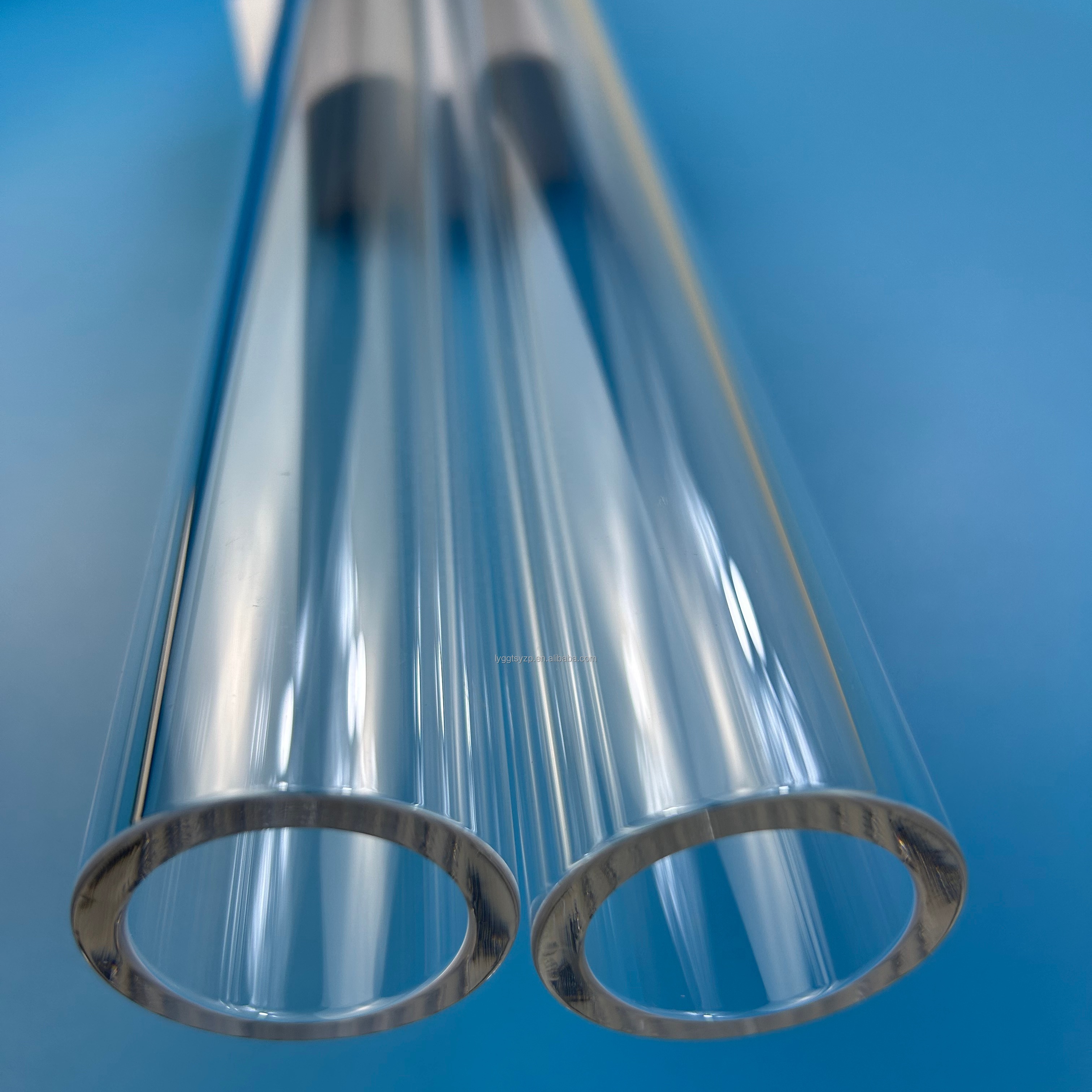
Polished Clear Quartz Twin Tube Ozone Free Heater Chemical Lab Equipment Semiconductor Furnace Tubes
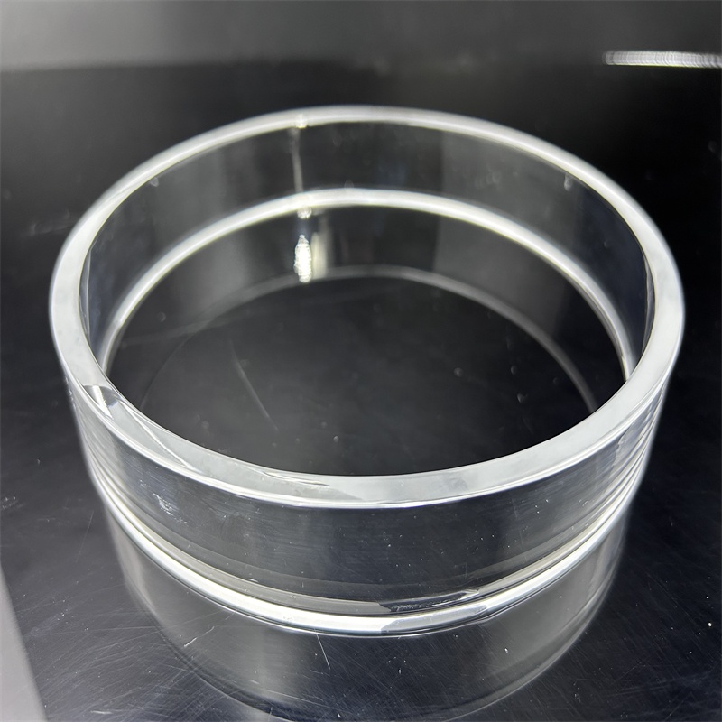
Customizable High Transparent Corrosion-resistant High Purity Fused Quartz Glass Bell Jar
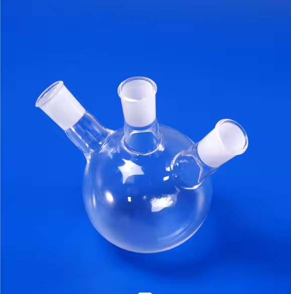
High Temperature Resistance Transparent Quartz Glass Twin Tube Bottom Flask
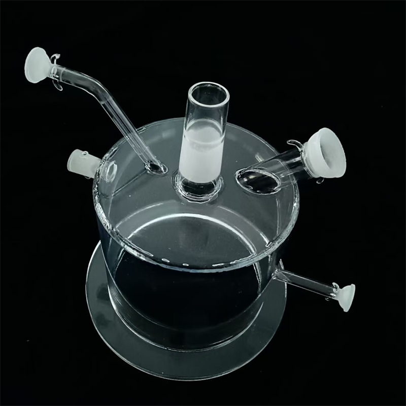
Customized High Pressure Clear Quartz Glass Tube Bending/Welding/Cutting 99.99% Pure Quartz
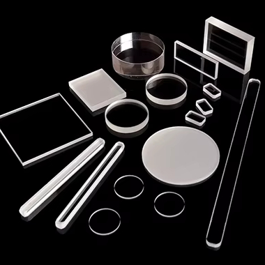
Custom Size High Temperature Fused Transparent Quartz Glass Optical Grade Test Sample Sheet
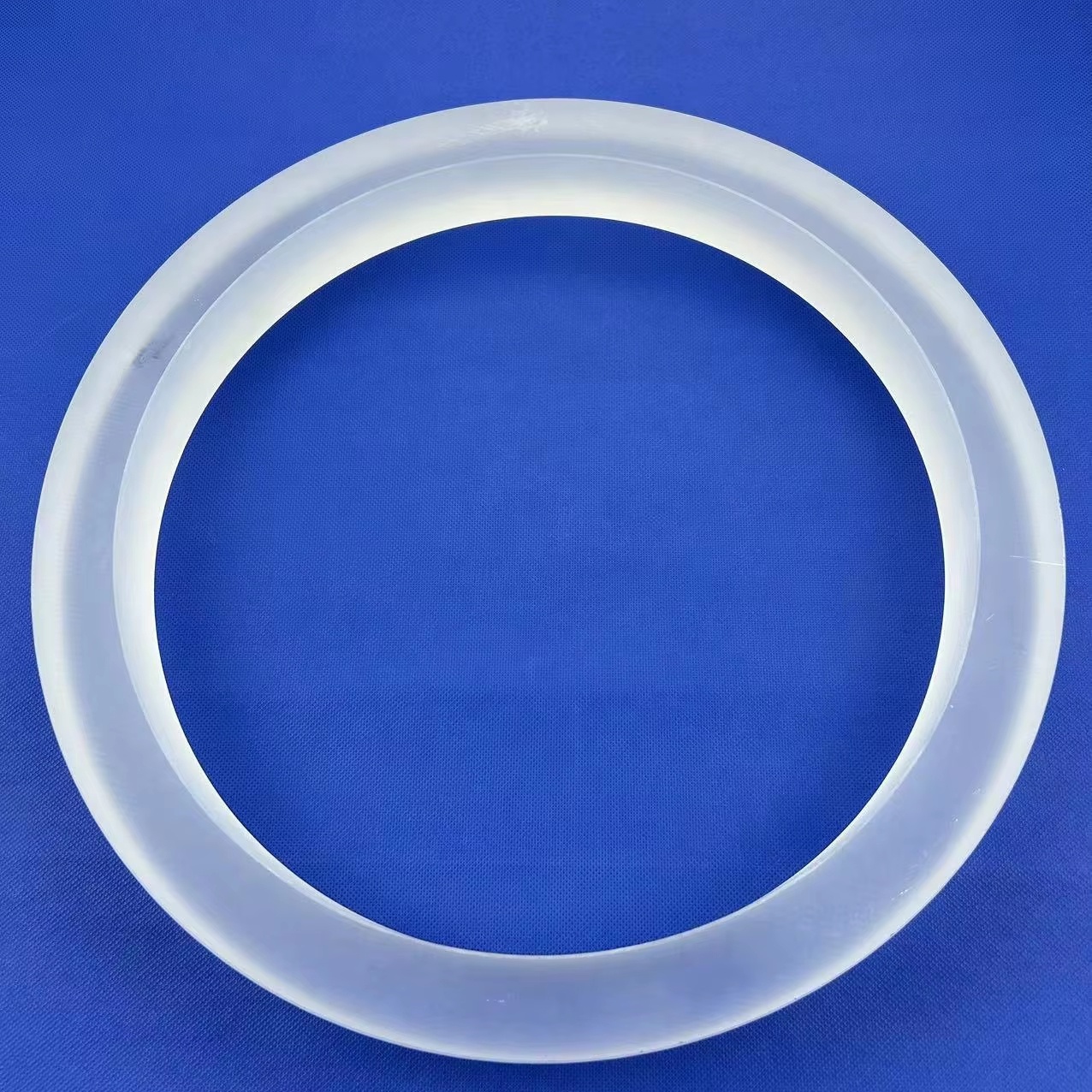
Custom Coated 99.99% Pure Quartz Rings for Semiconductor CVD Optics Applications
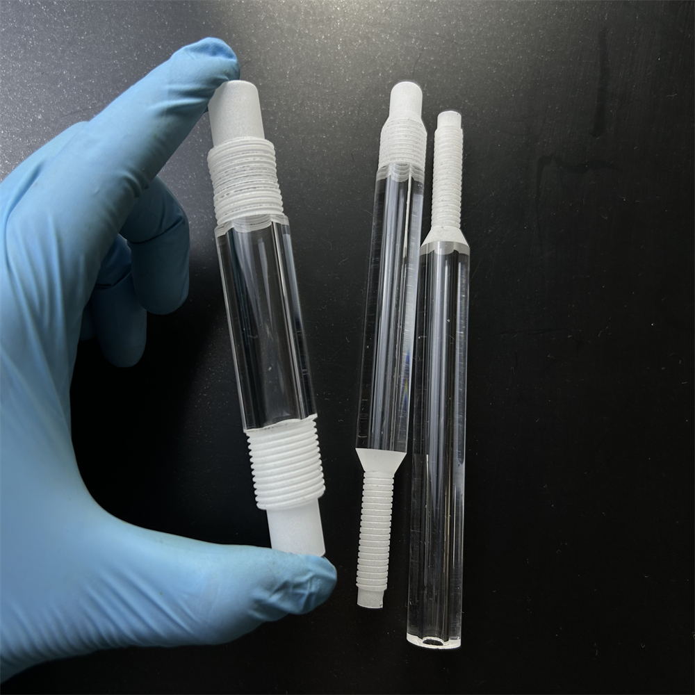
Customized High Purity Threaded Transparent UV Quartz Glass Tube with Precision Threading
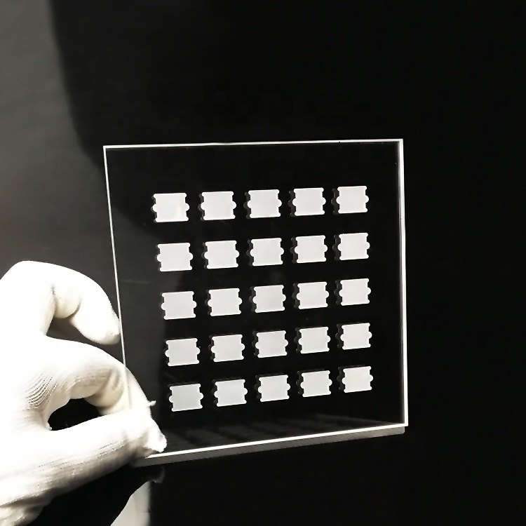
Factory Custom Fused Quartz Glass Circular High Quality XRD Sample Holder Optics Clear
Precision Quartz Carriers & High-Temperature Boats in Advanced Spanish Cleanrooms
Addressing the rigorous metallurgical, structural, and thermal stability requirements demanded by semiconductor R&D fabs, nanophotonics clusters, and power electronics pilot lines in the Autonomous Community of Madrid.
As the Madrid metropolitan area rapidly accelerates its microelectronics and photonic fabrication capability under the national PERTE Chip framework and European Chips Act, production and research cleanrooms face stringent hardware criteria. The performance of critical front-end thermal processes—including high-temperature atmospheric diffusion (phosphorus and boron dopant driving), gate oxide synthesis, low-pressure chemical vapor deposition (LPCVD), and rapid thermal annealing (RTA)—relies directly on the structural reliability and ultra-low ionic contamination of semiconductor quartz boats.
A semiconductor quartz boat is not merely a glass carrier; it is a critical process consumable operating at the thermodynamic limits of fused silica. When silicon or wide-bandgap (SiC, GaN) substrates undergo thermal cycles exceeding 1100°C, any mechanical distortion, dimensional sag, or molecular contamination within the quartz lattice propagates directly into batch-wide wafer failure. Thermal stress can provoke slip lines across the wafer substrate, while metallic impurities such as alkali ions (Na+, K+) or heavy transition metals (Fe, Cu, Ni) cause gate-oxide breakdown and severe carrier-lifetime degradation.
Sub-PPM Metallics
Fabricated using natural crystal raw materials with total trace metallic impurities strictly controlled to below 15–20 ppm, ensuring zero dopant migration into active wafer channels during high-temperature cycles.
Devitrification Resistance
Hydroxyl [OH⁻] content is managed within optimized windows (down to <5 ppm for JGS3 or controlled levels in JGS1) to elevate the viscosity annealing point and prevent premature quartz surface crystallization.
Laser Micro-Grooving
High-precision 5-axis CNC diamond grinding and laser-machined wafer slots guarantee slot-pitch accuracy within ±0.05 mm, preventing friction micro-scratches and automated robot transfer chattering.
In Madrid's specialized pilot labs—such as those operating within the Instituto de Sistemas Optoelectrónicos y Microtecnología (ISOM-UPM) and cleanrooms across Tres Cantos, Leganés, and Getafe—process flexibility is paramount. Wafers vary from standard 100 mm (4-inch) and 150 mm (6-inch) silicon discs to fragile compound semiconductors such as Indium Phosphide (InP), Gallium Arsenide (GaAs), and Silicon Carbide (SiC). Custom-engineered wafer boats must exhibit zero micro-crack initiation at welded rod junctions, requiring multi-pass hydrogen-oxygen flame fusion and thermal de-stressing annealing at 1215°C.
Fused Quartz Material Properties & Structural Tolerances
Engineered to exceed SEMI standards. Below is the technical baseline comparison verified via ICP-MS analysis and optical interferometry for quartz carriers supplied to European clients.
| Characteristic / Parameter | High-Purity Thermal Quartz (Carrier Boats) | Synthetic Fused Silica (JGS1 Grade) | Inspection Standard / Method |
|---|---|---|---|
| SiO2 Purity Content | ≥ 99.995% (4N5) | ≥ 99.999% (5N) | ICP-OES / ICP-MS Chemical Assay |
| Trace Metals (Fe, Cu, Ni, Na, K) | ≤ 8.0 ppm Total | ≤ 0.5 ppm Total | Spectrometric Trace Ion Measurement |
| Continuous Working Temperature | 1100 °C | 1150 °C | ASTM C965 Viscosity Curve Analysis |
| Maximum Short-Term Limit | 1300 °C | 1350 °C | Deformation Softening Point Testing |
| Softening Point (log η = 7.6) | approx. 1683 °C | approx. 1730 °C | Dilatometric Softening Assessment |
| Annealing Point (log η = 13.0) | approx. 1215 °C | approx. 1220 °C | Beam Bending Viscometry |
| Coefficient of Thermal Expansion (CTE) | 5.5 × 10⁻⁷ / °C (20–320°C) | 5.2 × 10⁻⁷ / °C | Interferometric Thermal Dilatometry |
| Slot Pitch Tolerance | ± 0.05 mm | ± 0.03 mm | Contact CMM & Non-Contact Optical Profiling |
| Surface Finish (Slot Internal Wall) | Fire-Polished / Ra ≤ 0.2 µm | Optical Super-Polish / Ra ≤ 0.05 µm | Stylus Profilometry & AFM Scan |
Madrid Cleanroom Applications & Specialized Use Cases
Tailored component configurations optimized for the research corridors, university cleanrooms, and industrial electronics plants across Madrid and central Spain.
Tres Cantos Space & Defense Optics
Supply of low-hydroxyl horizontal quartz boats and high-vacuum bell jars tailored for microchip assemblies and infrared sensors deployed in European Space Agency (ESA) aerospace projects situated along the M-607 tech corridor.
ISOM & UPM Microelectronics Fabs
Custom-spaced vertical wafer ladders engineered for experimental compound semiconductor dopings (GaN-on-Si and InP) requiring zero cross-contamination and exceptional dimensional stability up to 1250°C.
Leganés & Getafe Industrial Clusters
Heavy-duty, thick-walled transparent quartz reaction tubes and ozone-free twin heating cartridges designed for high-throughput thermal curing, optical fiber preform sintering, and industrial vacuum furnace operations.
CSIC Nanotechnology Infrastructure
Precision XRD sample holders, high-aspect optical discs, and laser-slotted micro-boats facilitating crystallographic defect analysis and non-destructive material characterization in cutting-edge nanotech laboratories.
Power Electronics & EV Inverters
Wide-diameter quartz furnace liners and customized high-pressure combustion flasks capable of sustaining extended thermal dwell intervals during Silicon Carbide (SiC) high-voltage diode thermal activation cycles.
Biomedical Microfluidic Prototyping
Deep-UV transparent JGS1 synthetic silica test substrates and micro-machined capillary carriers assisting Madrid's pharmaceutical and biotechnology clusters with high-temperature biochemical synthesis.
Macro Trend: The Strategic Impact of Spain's PERTE Chip on Consumable Sourcing
The Spanish government’s multi-billion euro PERTE Chip (Proyecto Estratégico para la Recuperación y Transformación Económica en Microelectrónica y Semiconductores) is shifting regional procurement strategies. Madrid is positioning itself as a central design and packaging node. As new pilot lines and pilot fabs emerge, local process engineers face long lead times (frequently exceeding 26–36 weeks) from legacy domestic or European quartz fabricators. Partnering with a vertically integrated Donghai manufacturer allows Madrid facility managers to compress delivery horizons down to 3–4 weeks for custom-machined carrier prototypes without compromising SEMI E1-grade material cleanliness.
Why Madrid Engineers Rely on Zunex Quartz
Combining raw material hegemony in China's Silicon Basin with international export standards, rapid turnaround, and direct engineering-to-engineering collaboration.
Direct CAD / Drawing Fabrication
We work directly from customer PDF, DWG, and 3D STEP models. Every drawing is screened by an optical quartz engineer to confirm thermal expansion compliance, fire-polish radii, and dimensional machinability before quotation.
Ultra-Clean Export Crating
Fragile quartzware ships to Madrid via shock-isolated wooden flight cases lined with custom ESD foam. Nitrogen-purged vacuum packaging prevents moisture adsorption and ionic particulate attraction during air transit into Adolfo Suárez Madrid-Barajas Airport (MAD).
Comprehensive QA & Traceability
Each delivery includes certificates of analysis (CoA) for raw crystal purity, optical transmission charts, and 3D coordinate measurement machine (CMM) inspection reports documenting wafer slot perpendicularity and runout.
Frequently Asked Questions by Madrid Specifiers
Clear answers addressing customs logistics, tariff handling, drawing tolerances, and chemical compatibility for buyers based in Spain.
How are customs clearance and VAT handled when shipping quartzware to Spain?
What wafer carrier slot tolerances can you guarantee for robotic end-effectors?
Can you manufacture custom diffusion boats for non-standard or small-batch substrates?
How does the quartz boat perform when cleaned with Hydrofluoric Acid (HF) baths?
What is the turnaround time from initial drawing submission to delivery in Madrid?
How do you prevent quartz devitrification during continuous 1100°C+ runs?
Request an Engineering Review & Quotation for Your Cleanroom
Upload your 2D drawings (PDF/DWG) or 3D models (STEP). Our semiconductor quartz specialists evaluate geometric tolerances, material purity grades, and delivery schedules to Madrid within two hours.