Engineered Quartz & Fused Silica Substrates Available for Rome
Direct OEM manufacturing compliant with ISO 9001 precision tolerances, laser drilling, micro-machining, and high chemical purity down to ≥99.99% SiO₂.
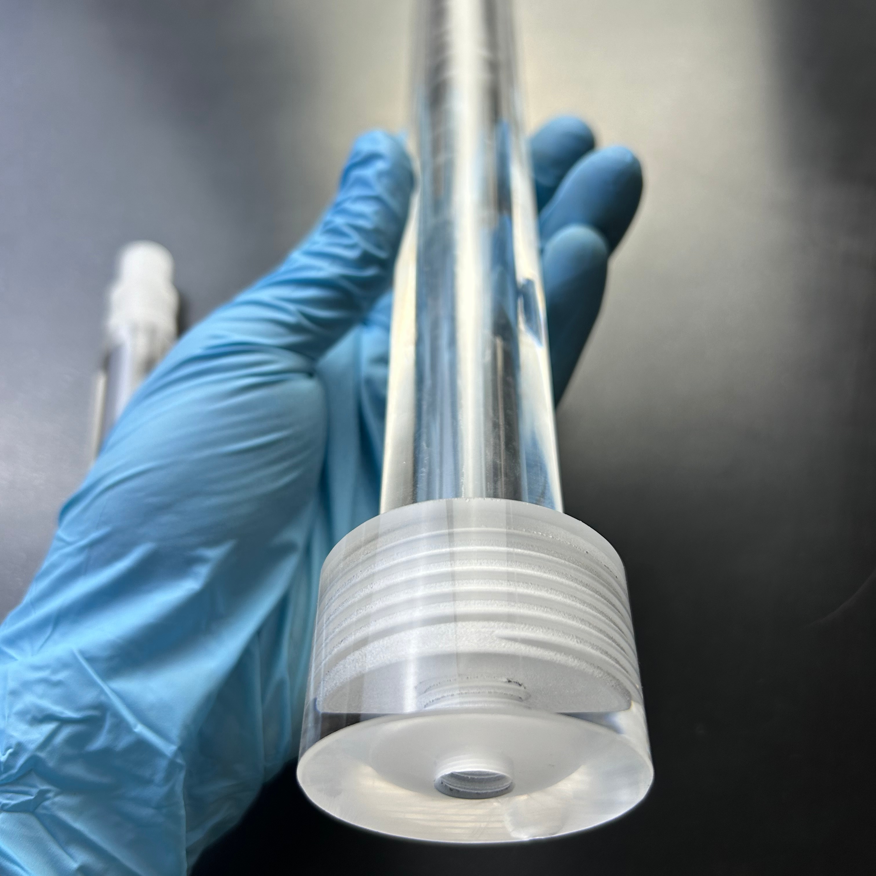
Customizable High Pressure Twin Quartz Tube
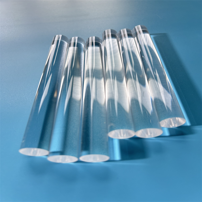
Optical Quartz Light Guide Cylinder Rod
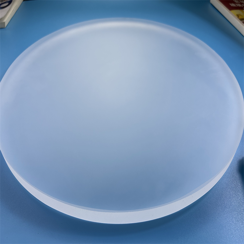
Frosted Quartz Substrate Disc & Plate
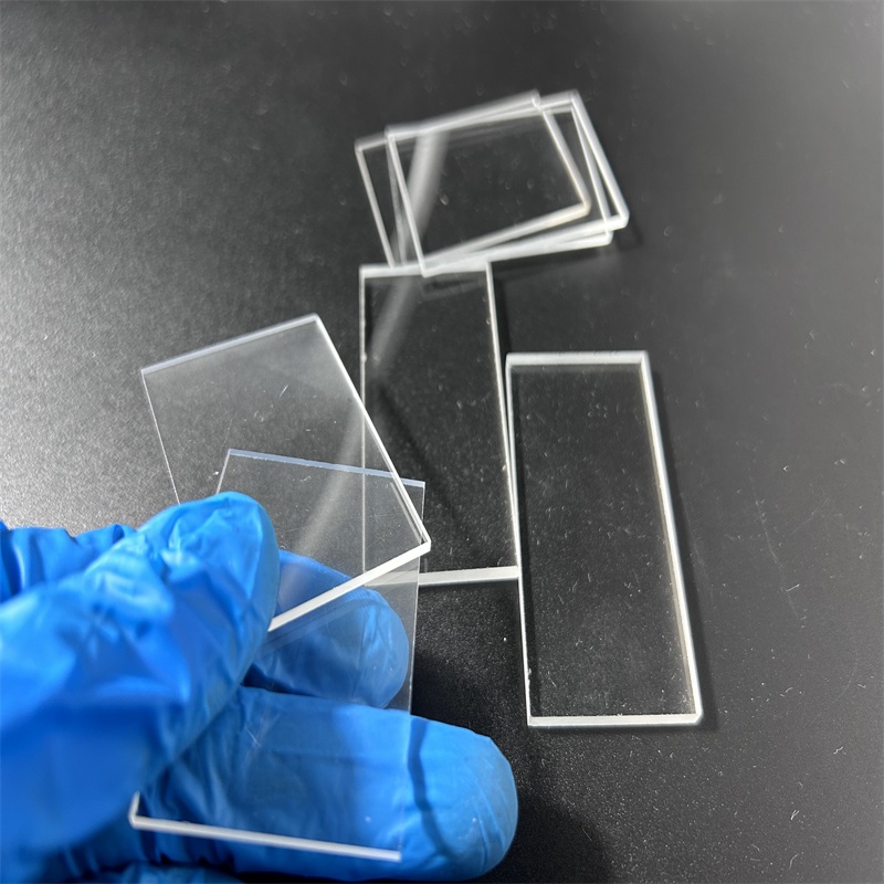
Optical Fused Quartz Substrate Sheet
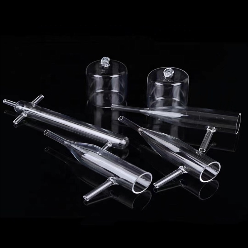
Laboratory CVD Furnace Quartz Twin Tube
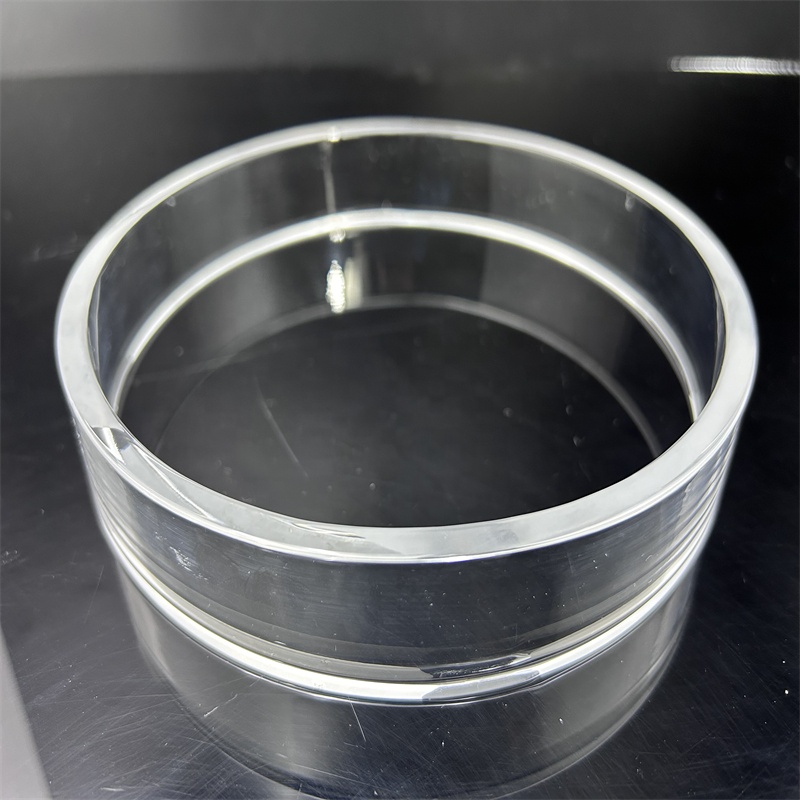
Corrosion-Resistant Quartz Bell Jar
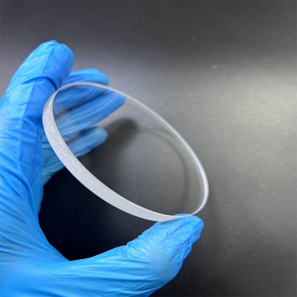
Precision Fused Silica Wafer Substrate
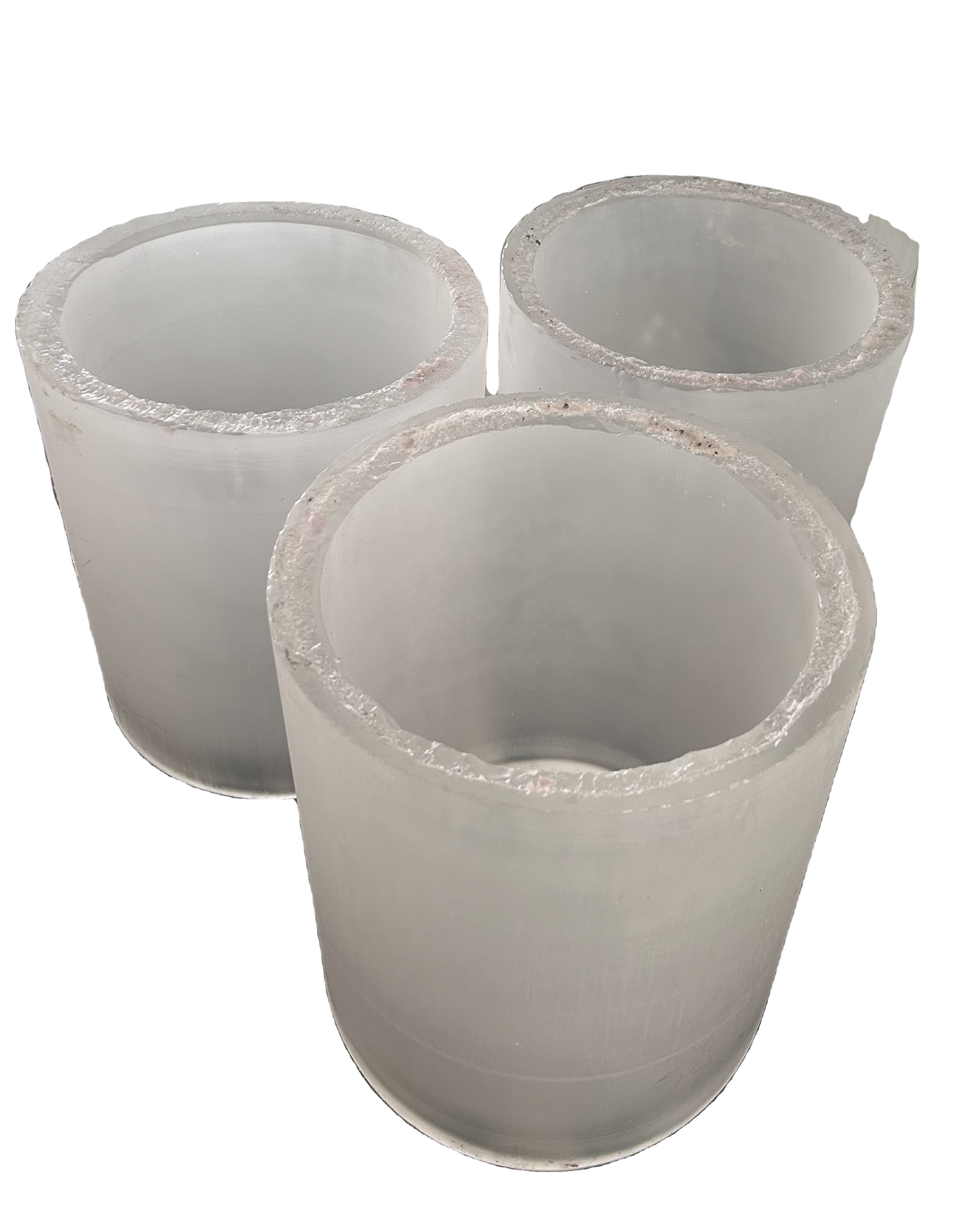
Fused Quartz Optical Cylinder Ingot
Supplying Fused Silica Substrates to Rome's Advanced Science & Defense Corridors
The metropolitan area of Rome and the wider Lazio region represent one of Southern Europe's most concentrated clusters for high-frequency telecommunications, optoelectronics, aerospace engineering, and nuclear quantum physics. From the research campuses along the Via Tiburtina (Tecnopolo Tiburtino) to the aerospace conglomerates operating in the Lazio Aerospace Cluster (DTA), procurement teams require reliable access to precision-engineered fused silica substrates with verified isotopic and chemical purity.
Synthetic fused silica substrates are chemically synthesized using silicon tetrachloride (SiCl₄) oxidation, resulting in material structures nearly free of metallic contaminants (<0.1 ppm Fe, Al, Ti). For Roman microfabrication cleanrooms, biomedical photonic developers, and satellite communication payloads, these substrates deliver non-fluorescing UV-C transparency down to 185 nm, minimal wavefront distortion (λ/10 per inch), and exceptional thermal stability with a near-zero coefficient of thermal expansion (5.5 × 10⁻⁷/°C).
- Sub-nanometer surface roughness (Ra < 0.5 nm)
- Total Thickness Variation (TTV) < 1.5 μm
- Laser damage threshold > 15 J/cm² @ 1064nm
- Full compliance with EU RoHS & REACH directives
Substrate Grade Selection Spectrum
JGS1 (Synthetic Deep-UV Fused Silica)
Transmission band 185 nm – 2500 nm. Virtually bubble-free, OH content ~1200 ppm. Ideal for excimer lithography, UV laser windows, and DUV bio-chips in Roman scientific laboratories.
JGS2 (Optical Grade Fused Quartz)
Transmission band 220 nm – 2500 nm. Produced by electric fusion of natural high-purity quartz crystal. Highly resistant to high-temperature thermal cycling up to 1100°C continuous.
JGS3 (Infrared Water-Free Fused Silica)
Transmission band 260 nm – 3500 nm. Vacuum electro-fused with residual OH < 5 ppm. Eliminates absorption bands at 2.73 μm, essential for IR aerospace viewports and FLIR calibration.
Specialized Applications Across Rome & Central Italy
Strategic deployment of precision fused silica substrates in critical engineering clusters throughout Rome and Lazio province.
Aerospace Payloads & Star Trackers (Rome-Castel Romano)
Aerospace integrators in the greater Rome area require ultra-stable optical substrates for satellite Earth-observation cameras, star tracker baffles, and deep-space spectrometers. Fused silica's extreme dimensional stability across orbital temperature swings (-100°C to +150°C) prevents focal point drift and optical astigmatism under vacuum conditions.
Quantum Photonics & INFN Particle Physics (Frascati Belt)
Located immediately outside Rome, research hubs such as the National Institute for Nuclear Physics (INFN) and CNR laboratories implement fused silica optical flats, beam splitters, and vacuum viewports for ultra-fast laser-plasma acceleration and quantum entanglement interferometry, where zero internal stress birefringence is non-negotiable.
Semiconductor Cleanrooms & MEMS (Tecnopolo Tiburtino)
Electronic foundries along the Via Tiburtina corridor utilize high-pressure fused silica wafers as carrier substrates for fragile compound semiconductors (GaN, InP, SiC) and high-aspect-ratio MEMS micro-machining. Low dielectric loss (ε = 3.78 @ 1 MHz) makes fused silica the definitive substrate for RF micro-switches and radar antennas.
Market Evolution & Sourcing Realities in Italy
How European semiconductor sovereignty initiatives and Italian manufacturing modernization are reshaping fused silica substrate specifications.
European Chips Act Alignment
Rome-based photonics developers are aligning their pilot lines with EU-funded pilot fabricators. This migration necessitates rigorous wafer provenance, lot-to-lot trace certificates, and certified DIN/ISO cleanroom vacuum packaging to integrate smoothly into automated EU handling tools.
Sub-Micron Laser Finishing
Italian engineers increasingly replace mechanical diamond grinding with ultra-short pulse picosecond and femtosecond laser processing. This eliminates edge chipping, minimizes micro-crack depth under 5 μm, and allows intricate blind holes and fluidic micro-channels.
High-Power Laser Resilience
With Lazio serving as a prime Italian hub for industrial laser cutting and defense directed-energy research, procurement teams demand bulk synthetic silica substrates that exhibit ultra-low optical absorption (<3 ppm/cm @ 1064 nm) to prevent thermal lensing and beam distortion.
Direct Factory Air Express
Bypassing multiple domestic reseller margins in Italy, Roman institutes now source directly from our manufacturing facility in Donghai, securing factory-grade pricing, direct CAD-to-CNC validation, and door-to-door delivery to Rome Fiumicino (FCO) within 5 to 7 business days.
Fused Silica Substrate Performance Benchmarks
Empirical mechanical, electrical, and optical properties verified under metrological testing for industrial and scientific buyers.
| Physical / Optical Parameter | JGS1 (Synthetic Silica) | JGS2 (Optical Quartz) | JGS3 (Infrared Silica) | Test Standard / Metrology |
|---|---|---|---|---|
| Transmission Spectrum | 185 nm – 2500 nm (DUV) | 220 nm – 2500 nm (Standard) | 260 nm – 3500 nm (NIR/MIR) | Spectrophotometer UV-Vis-NIR |
| SiO₂ Chemical Purity | ≥ 99.999% | ≥ 99.99% | ≥ 99.995% | ICP-MS Trace Analysis |
| Hydroxyl (OH) Content | ~ 1200 ppm (High OH) | 150 – 300 ppm | < 5 ppm (Water-free) | FTIR Absorption Spectrum |
| Density @ 20°C | 2.201 g/cm³ | 2.203 g/cm³ | 2.200 g/cm³ | ASTM C693 Archimedes |
| Thermal Expansion (0–300°C) | 5.5 × 10⁻⁷ / °C | 5.5 × 10⁻⁷ / °C | 5.4 × 10⁻⁷ / °C | Dilatometry ISO 7991 |
| Softening Point | 1730 °C | 1683 °C | 1710 °C | ASTM C338 Fiber Elongation |
| Surface Roughness (CMP) | Ra ≤ 0.3 nm | Ra ≤ 0.5 nm | Ra ≤ 0.4 nm | Atomic Force Microscopy (AFM) |
| Refractive Index (nd @ 587.6nm) | 1.45846 | 1.45850 | 1.45840 | V-Block Refractometer |
| Dielectric Constant (1 MHz) | 3.78 | 3.80 | 3.77 | ASTM D150 Impedance Analysis |
| Laser Damage Threshold (1064nm, 10ns) | > 20 J/cm² | > 12 J/cm² | > 18 J/cm² | ISO 21254 Pulsed Laser Protocol |
Precision Manufacturing & Quality Architecture
From raw high-purity chemical vapor boule synthesis to cleanroom final packaging, every order follows strict quality milestones.
Drawing & CAM
Technical assessment of STEP/DWG blueprints. Finite Element validation for edge break, slot tolerances, and optical apertures.
Wire Saw Slicing
High-precision diamond wire multi-slicing of boule ingots into blanks, guaranteeing minimal kerf loss and sub-10μm planarity.
Laser Micro-Machining
Precision laser drilling (ø ≥ 0.1 mm), contour routing, and edge beveling without thermal micro-fracturing or localized stress.
Double-Sided CMP
Chemical Mechanical Polishing yielding super-smooth finishes (Ra < 0.5 nm), 20/10 or 10/5 scratch-dig, and λ/10 flatness.
Ultrasonic Clean & Pack
Multi-stage deionized water ultrasonic wash, class 100 cleanroom vacuum seal, nitrogen purged, and crated for export to Rome.
Frequently Asked Questions by Buyers in Rome & Italy
Transparent technical, logistics, and commercial answers for institutional and corporate purchasing directors.
What are the lead times and shipping logistics from your facility to Rome?
For custom-machined fused silica substrates manufactured to drawing, typical production turnaround ranges from 7 to 14 business days depending on optical tolerance requirements (e.g., CMP polishing or laser-drilled hole arrays). Shipments to Rome and the central Italy region are routed via prioritized air courier (DHL Express, FedEx International Priority, or air freight directly to Rome Fiumicino Airport - FCO), taking 3 to 5 business days in transit. We furnish real-time tracking numbers and handle all export clearance paperwork.
How do you handle Italian customs clearance, EORI, and VAT (IVA) compliance?
We routinely supply academic institutions (e.g., Sapienza Università di Roma, Tor Vergata), research entities (CNR, INFN), and private aerospace corporations throughout Italy. Commercial invoices provide exact HS codes (such as 7002.31 for fused quartz tubes/rods and 7006.00 / 9001.90 for optical plates and substrates), precise gross/net weights, and country-of-origin documentation. Shipments can be delivered DDU/DAP to your facility or DDP where all Italian import customs formalities and local VAT (Imposta sul Valore Aggiunto) are pre-cleared by the global courier.
Can you supply wafer substrates compliant with SEMI standards (flat or notch)?
Yes. We manufacture standard 2-inch, 3-inch, 4-inch, 6-inch, 8-inch, and 12-inch fused silica and quartz glass wafers in full conformance with SEMI specifications. Substrates feature precision orientation flats (primary and secondary) or laser-cut SEMI-standard alignment notches. Thicknesses range from ultra-thin 100 μm up to standard 500 μm, 725 μm, or custom millimeter-scale plates, with total thickness variation (TTV) tightly managed below 2 μm.
What documentation and metrology certificates accompany the substrate shipments?
Every export batch sent to Italy includes a comprehensive Certificate of Analysis (CoA) containing ICP-MS trace metal analysis, optical transmission spectral curves across target wavelength bands, Zygo interferometry reports verifying surface flatness (λ/10 to λ/20), and mechanical CMM dimensional verification data. RoHS, REACH, and conflict-mineral compliance statements are generated for institutional audit trails.
How do you protect fragile quartz substrates against shock and contamination during transport?
Optical grade plates and polished wafers are individually packed in class 100 cleanroom-compatible wafer cassettes or gel-boxes with non-outgassing surface membranes that hold the optics suspended without surface contact. These primary carriers are hermetically vacuum-sealed inside antistatic, nitrogen-purged moisture-barrier bags. Outer packaging features multi-layered high-density EPE shock absorption foam, impact indicators, and export-grade reinforced wooden crates compliant with ISPM-15 heat-treatment standards.
Why Italian Engineers & Specifiers Partner With Us
Rooted in China's quartz capital Donghai, combining direct industrial processing scales with rigorous European precision expectations.
In-House Laser Finishing
Proprietary multi-axis CNC quartz laser drilling, internal slotting, and flame fire-polishing stations deliver flawless contours and high edge strength without structural micro-fissuring.
Custom CAD/CAM Slicing
Direct translation from client CAD models (DWG, DXF, STEP) to machine toolpaths. We accommodate low-volume research prototypes up to recurring monthly production batches.
Under 2-Hour Quotations
Our verified response rate is 100% with average technical reply times under two hours. Optical engineers evaluate your tolerances, edge chamfers, and grade criteria immediately.
Verified Supplier Pedigree
Backed by a 43% repeat-order rate from international B2B buyers and fully audited financial and trade capacity data (US$2.5M - US$5M annual export volume).
Request a Technical Quotation for Rome & Central Italy Delivery
Submit your CAD drawing, target dimensions, surface roughness (Ra), and material grade (JGS1, JGS2, JGS3). Our engineering team will review manufacturability, verify tolerances, and provide a competitive factory quotation with guaranteed door-to-door delivery schedules.