Specialized Fused Quartz Glass Solutions for High-Precision Applications
Direct from our specialized crystal and quartz processing center in Donghai to Eindhoven’s advanced semiconductor, photonic, and industrial vacuum clusters.
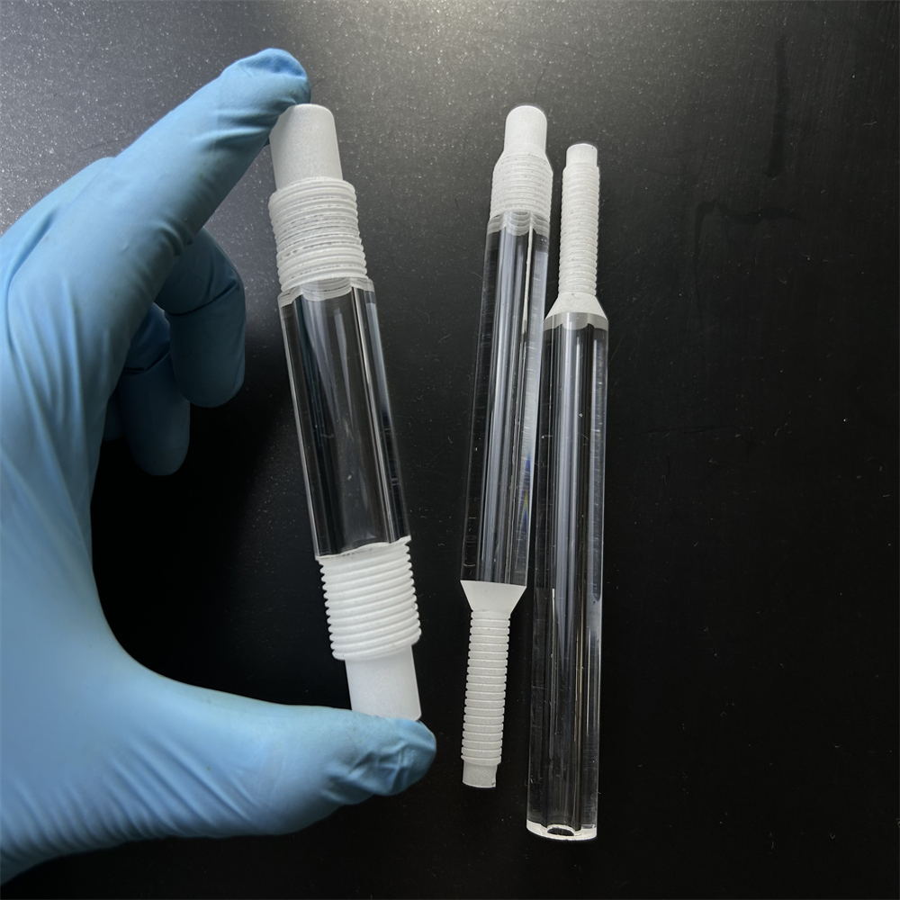
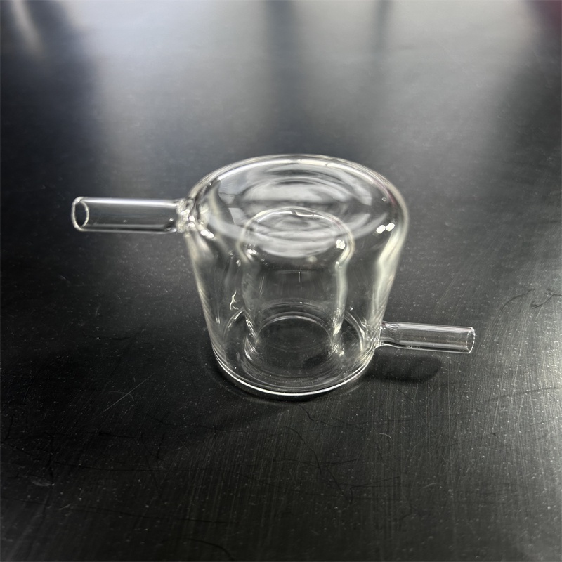
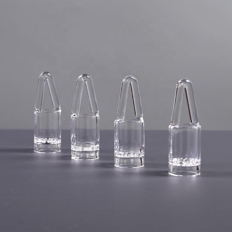
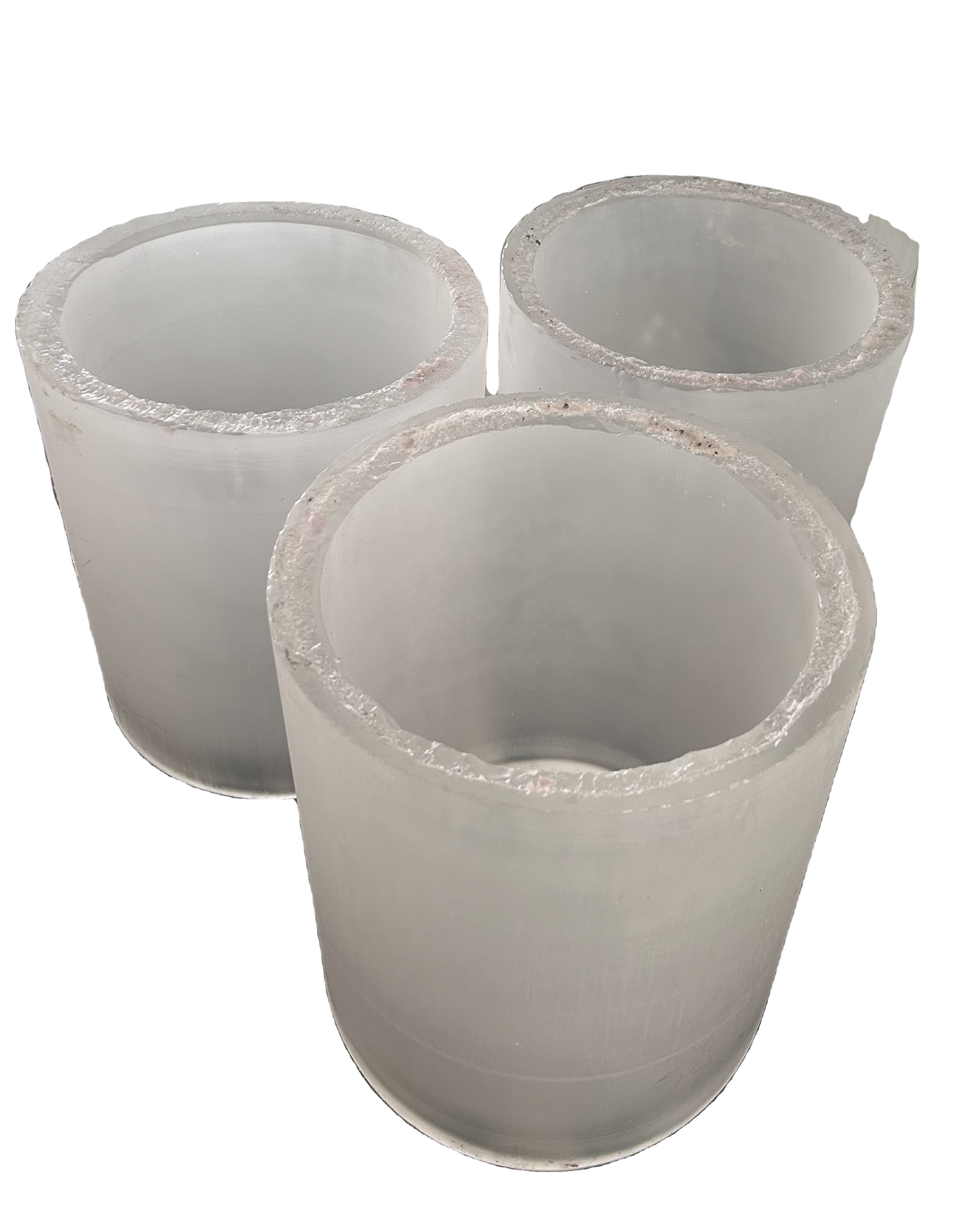
Precision Fused Quartz Glass in the Brainport Eindhoven Advanced Engineering Matrix
Eindhoven, situated in the North Brabant province of the Netherlands, serves as Europe’s epicenter for microelectronics, deep-submicron lithography, integrated photonics, and ultra-high vacuum (UHV) mechatronics. Driven by industry titans such as ASML, Thermo Fisher Scientific (FEI Electron Optics), VDL Enabling Technologies Group, and the research institutes at Eindhoven University of Technology (TU/e), the regional demand for high-grade synthetic fused silica and thermal fused quartz surpasses standard commercial parameters. Equipment designers require structural stability under 1100°C continuous thermal loads, near-zero coefficient of thermal expansion, extreme chemical inertness against fluorine-based plasmas, and structural zero-bubble optical clarity.
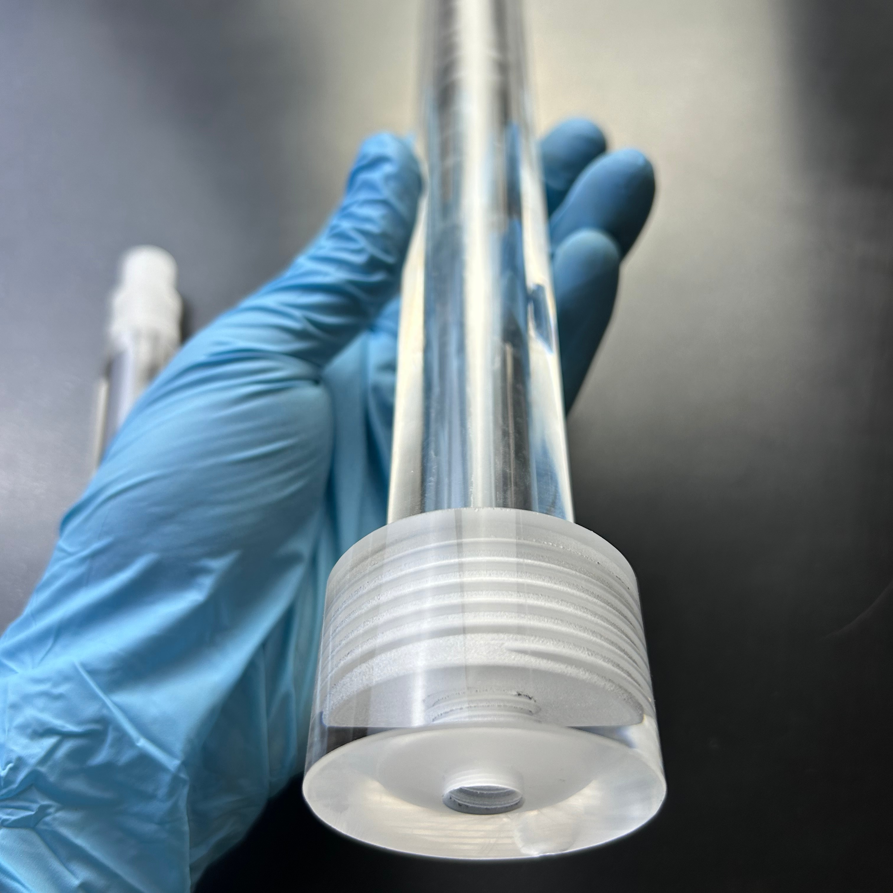
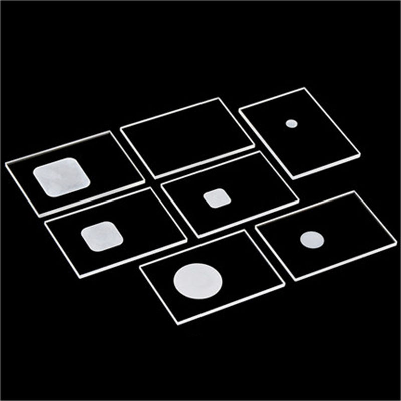
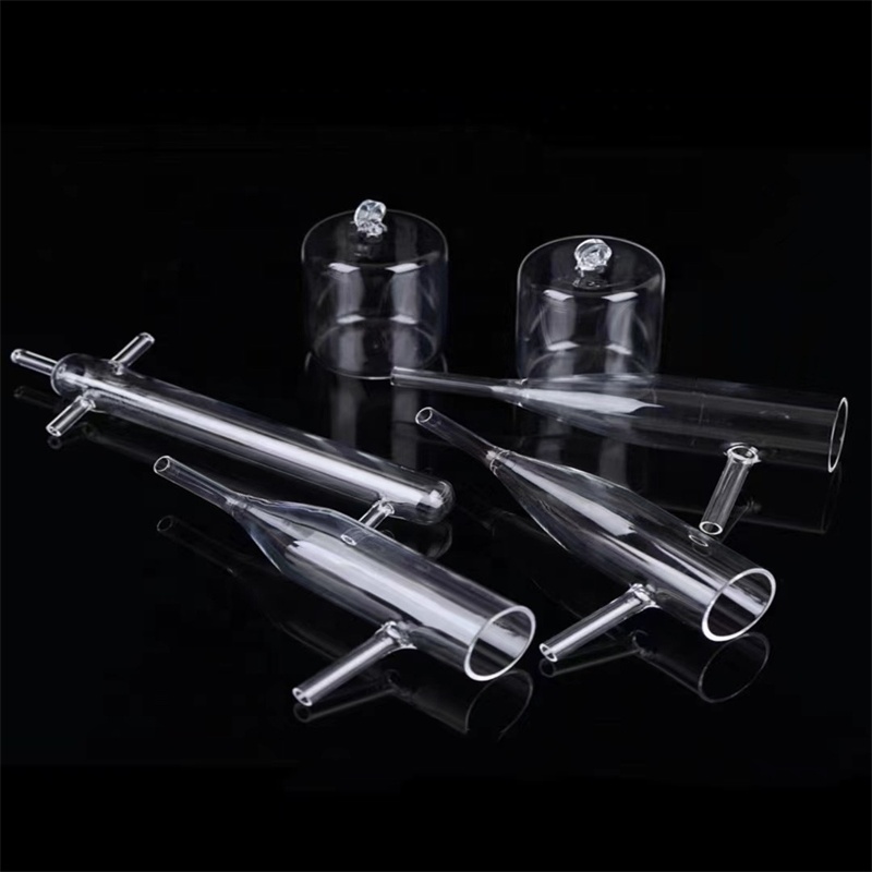
As a dedicated Chinese OEM/ODM manufacturer headquartered in Donghai County—the globally recognized "Crystal Capital" with raw silica reserves holding ≥99.99% purity—Zunex Quartz Products Co., Ltd. bridges high-capacity precision fabrication directly with Eindhoven’s equipment tier-1 and tier-2 supply chains. By integrating high-temperature flame fusion, multi-axis cold machining, surface laser polishing, and automated laser drilling/grooving, we deliver fully customized quartz tubes, polished optical windows, slotted wafer carriers, and twin-tube reactors directly matching European engineering standards (DIN, ISO 10110, and SEMI specifications).
| Material Property | JGS1 (Synthetic Fused Silica) | JGS2 (Optical Fused Quartz) | JGS3 (Infrared Fused Silica) |
|---|---|---|---|
| Primary Optical Transmission | 185 nm – 2,500 nm (Deep DUV/UV) | 220 nm – 2,500 nm (UV-VIS) | 260 nm – 3,500 nm (Near-to-Far IR) |
| Hydroxyl Ion (OH¯) Concentration | < 5 ppm – 1200 ppm (Grade Tuned) | ≤ 30 ppm – 150 ppm | ≤ 5 ppm (Water-Free IR Optimized) |
| Coefficient of Thermal Expansion (CTE) | 5.5 × 10⁻⁷ / °C (20°C to 320°C) | 5.5 × 10⁻⁷ / °C | 5.4 × 10⁻⁷ / °C |
| Softening & Annealing Points | 1,730 °C / 1,180 °C | 1,683 °C / 1,215 °C | 1,700 °C / 1,200 °C |
| Maximum Working Temperature | Continuous: 1,100°C | Peak: 1,300°C | Continuous: 1,100°C | Peak: 1,250°C | Continuous: 1,150°C | Peak: 1,350°C |
| Dielectric Strength (20°C, 1MHz) | 2.5 × 10⁷ V/m | 2.0 × 10⁷ V/m | 2.2 × 10⁷ V/m |
| Key Applications in Eindhoven | DUV/EUV beam inspection, optical flats | Wafer viewports, sight glasses, heaters | IR heating modules, CVD thermal chambers |
Localized Industrial Applications Across the Brainport Tech Corridor
Tailored manufacturing routes supporting high-vacuum, lithographic, chemical vapor deposition, and analytical processes across Brainport Eindhoven, Veldhoven, Best, and Helmond.
Semiconductor Subsystems & Wafer Handling
In the Veldhoven-Eindhoven cleanroom semiconductor cluster, quartz components form contamination-free process chambers. We produce custom-dimensioned slotted quartz boats, furnace process tubes, gas distribution injector rings, and wafer susceptors engineered with trace metal impurities under 1 ppm, preventing iron, sodium, or copper migration during high-temperature annealing.
Photonic Integrated Circuits & Optics
Eindhoven is home to Europe’s leading Photonic Integrated Circuit (PIC) ecosystem (PhotonDelta). We supply double-side optical polished JGS1 quartz flats, wave plates, precision prisms, and zero-fluorescence quartz cuvettes featuring surface roughness Ra < 0.5 nm and parallelism < 10 arcseconds for coupling alignment and laser-to-chip packaging arrays.
Industrial Twin-Tube IR Emitters
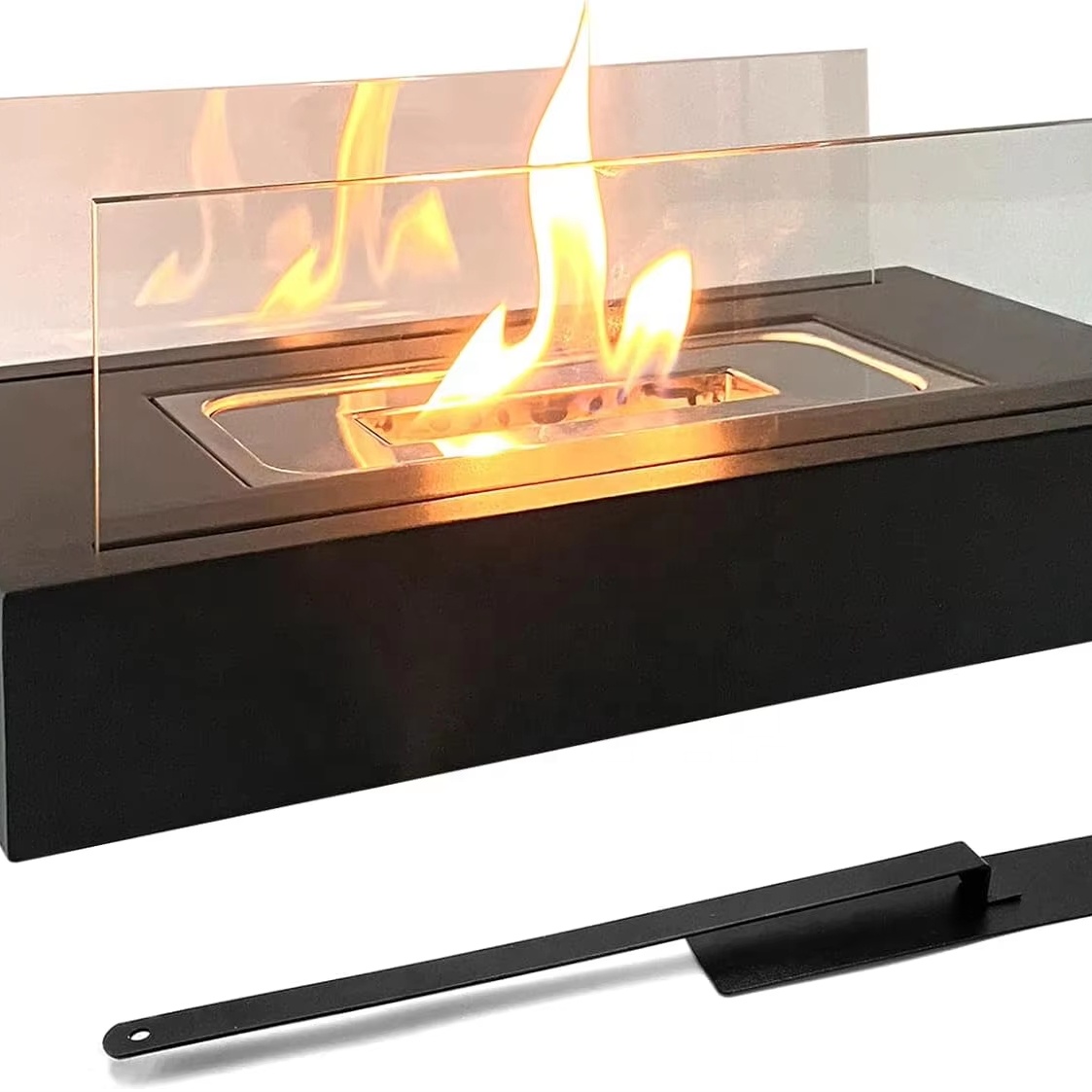
Advanced assembly lines in North Brabant utilize short-wave and medium-wave twin-tube infrared heaters for composite curing, plastic thermoforming, and solar cell metallization. Our custom 99.99% clear quartz twin-tubes offer exceptional mechanical rigidity against deflection under elevated pressure, coupled with gold or ceramic reflective coatings.
Analytical Testing, XRD & Electron Microscopy
With major electron microscope innovators located in the Eindhoven metropolitan district, diagnostic instruments demand pure quartz sample holders, XRD zero-background sample plates, and specialized plasma combustion ampoules capable of maintaining vacuum seals without outgassing under 10⁻⁶ Pa conditions.
Macro Trends Reshaping Fused Quartz Procurement in the Eindhoven High-Tech Ecosystem
The European Chips Act and aggressive private capital deployment into Eindhoven have established unprecedented benchmarks for raw material dependability and engineering documentation. Sourcing managers and R&D engineers are moving away from traditional broker channels in favor of vertically integrated manufacturing partners who satisfy three core requirements:
1. Zero-Contamination Cleanliness
Local assembly facilities in Eindhoven require quartzware cleaned through multi-stage ultrasonic deionized water cascades, certified acid etching (HF/HNO3 blend), and double vacuum heat-sealed cleanroom packaging conforming to Grade 2 cleanroom standards upon direct unpacking.
2. Laser Micro-Finishing
Traditional mechanical diamond grinding introduces micro-cracks along cut paths that propagate into thermal fractures under cyclic 1000°C operation. The rapid adoption of picosecond laser ablation and flame micro-polishing eliminates internal stress risers along precision apertures and slotted carriers.
3. De-risked Sourcing & CAD Autonomy
OEMs require rapid engineering turnaround: immediate manufacturability feedback on STEP/DWG native models, single-piece rapid prototyping for dynamic test benches, and seamless volume ramp-up backed by factory-direct capacity without distributor margin stack.
Factory-Direct Manufacturing Competencies for European Sourcing
Combining the mineral resource dominance of Donghai with stringent ASML-adjacent quality management.
Direct Sourcing in China's Crystal Hub
Operating directly in Donghai County, Jiangsu, Zunex controls raw material purity from the crystal refining stage. This regional supply concentration eliminates intermediate processing markups, ensures steady quartz ingot availability, and guarantees competitive pricing for custom OEM batch programs.
Advanced Laser & Hot-Working Capabilities
Our workshop integrates multi-axis CNC laser cutting, laser hole drilling down to Ø0.2 mm with negligible chipping (<0.05 mm), precision slotting for semiconductor wafer cages, high-precision lathe blowing, flanging, and fire-polishing to achieve smooth, stress-relieved optical finishes.
Engineered Response within ≤ 2 Hours
Technical collaboration is supported by degreed optical and materials engineers. Every Dutch RFQ containing technical drawings or STEP models receives comprehensive manufacturability reviews, tolerance feedback, and formal cost estimations within two hours, keeping rapid prototyping cycles agile.
Zero-Breakage Global Logistics to the Netherlands
Exporting fragile quartz requires meticulous engineering. We utilize custom high-density molded EPE foam beds, multi-wall hermetic inner boxes, and fumigated OSB plywood crates with integrated shock-watch indicators, delivering reliably via air express directly to Eindhoven Airport or Rotterdam DDP.
Verified Performance: 43% Repeat-Order Rate
With an annual revenue range between US$2.5M – US$5.0M and verified independent trade records on Alibaba.com, our transparent production line tracking and repeatable dimensional compliance drive a proven 43% buyer repeat order rate across demanding tech sectors.
Full Traceability & Material Certification
Every shipment is supported by comprehensive documentation: Certificate of Conformance (CoC), spectral transmission curves (UV-VIS-NIR), dimensional CMM inspection reports, and trace element spectrometry (ICP-MS) verifying heavy metal thresholds below critical parts-per-billion levels.
Frequently Asked Questions by Eindhoven Hardware & Process Engineers
Clear, definitive technical clarifications addressing thermal thresholds, chemical resistance, tolerances, and European delivery mechanics.
How do JGS1, JGS2, and JGS3 quartz types compare for DUV lithography vs. thermal furnace applications?
JGS1 is a synthetic fused silica produced by chemical vapor oxidation of silicon tetrachloride (SiCl4). It features virtually zero metallic impurities and absence of bubble inclusions, offering superior transmission (>90%) in the deep ultraviolet down to 185 nm. This makes JGS1 mandatory for laser viewports, lithography projection optics, and UV exposure masks. JGS2 is manufactured by fusing natural quartz crystal sand; it transmits well in the 220–2,500 nm range and provides optimal cost-performance for thermal diffusion tubes, sight windows, and CVD chambers. JGS3 is melted under vacuum with special de-hydroxylation processing to bring residual OH¯ down below 5 ppm, eliminating the characteristic 2.73 μm water absorption band, making it the premier choice for infrared twin-tube heating elements and broadband IR sensors.
What mechanical and dimensional tolerances can you sustain on custom machined quartz tubes and plates?
For CNC cold-machined optical plates, discs, and windows, our standard machining tolerance is ±0.05 mm, with precision CNC lapping and polishing achieving ±0.01 mm on dimensions and ±0.005 mm on thickness. Surface flatness can be controlled down to λ/4 or λ/10 per 25 mm diameter, with scratch-dig standards conforming to MIL-PRF-13830B (20/10 or 40/20). For hot-worked fused quartz tubes (OD > 100 mm), outside diameter and wall thickness tolerances are typically maintained within ±1.0% to ±0.5% via automated laser caliper measurement systems during tube redrawing.
How does high-purity fused quartz behave under aggressive chemical environments like HF or plasma etching?
Fused quartz shows extraordinary chemical inertness: it is resistant to water, concentrated saline solutions, and all organic/inorganic acids at room and elevated temperatures, with the sole exceptions of hydrofluoric acid (HF) and hot concentrated phosphoric acid (>150°C). Under fluorine-based plasma etching (CF4, SF6, NF3) commonly employed in Dutch wafer fabrication, fused quartz gradually erodes forming volatile SiF4 gas. However, due to its low trace-metal profile (<1 ppm alkali metals), our high-purity quartz erodes homogeneously without producing micro-particulate flaking or metal ion redeposition on substrate surfaces.
What is the procedure for rapid prototyping and transition to recurring batch supply for Eindhoven OEMs?
Upon receiving your engineering package (PDF, STEP, or DWG) with specified operating parameters and tolerance callouts, our engineering department reviews the model and returns a DFM (Design for Manufacturability) analysis alongside a firm quotation within 2 hours. Prototype fabrication typically takes 5 to 10 working days depending on laser machining and optical polishing complexity. Once initial parts pass first-article inspection (FAI) in Eindhoven, we lock the CNC tool paths, fixture parameters, and raw material batch codes to guarantee exact repeatability for recurring scheduled production runs.
What logistics frameworks, incoterms, and customs procedures apply to shipments entering the Netherlands?
We routinely support DDP (Delivered Duty Paid), DAP, and CIF terms directly to Eindhoven business parks (Flight Forum, High Tech Campus, De Run, and Esp). Urgent engineering prototypes and low-volume batches ship via DHL Express or FedEx Air, clearing Amsterdam Schiphol (AMS) and arriving in Eindhoven within 3 to 5 business days. Heavy furnace process tubes, large-diameter quartz tanks, and production-volume twin-tubes are freighted via air pallet or maritime container into the Port of Rotterdam, supported by complete HS code classification (typically 7002.31 for quartz tubes, 7006.00 for worked plates), EUR.1 customs documentation, and commercial invoices.
Collaborate with Our Precision Quartz Engineering Team
Accelerate your semiconductor, vacuum, or photonics project in Eindhoven with high-purity fused silica and quartz ware fabricated exactly to your drawing tolerances. Direct factory pricing, certified material compliance, and 2-hour technical quoting.
Contact Us