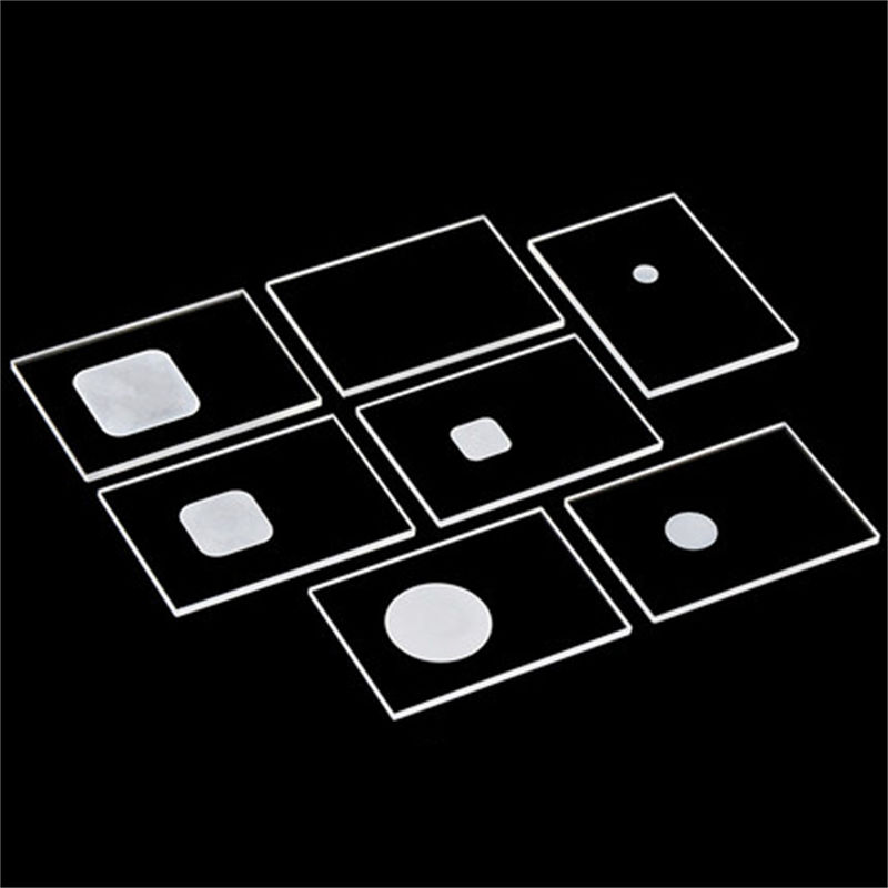
Specialized Fused Quartz Components Ready for Export
Every substrate, disc, and tube is manufactured in Donghai under strict ISO protocols, featuring CNC ultra-fine edging, laser micro-machining, and certified spectrographic purities.
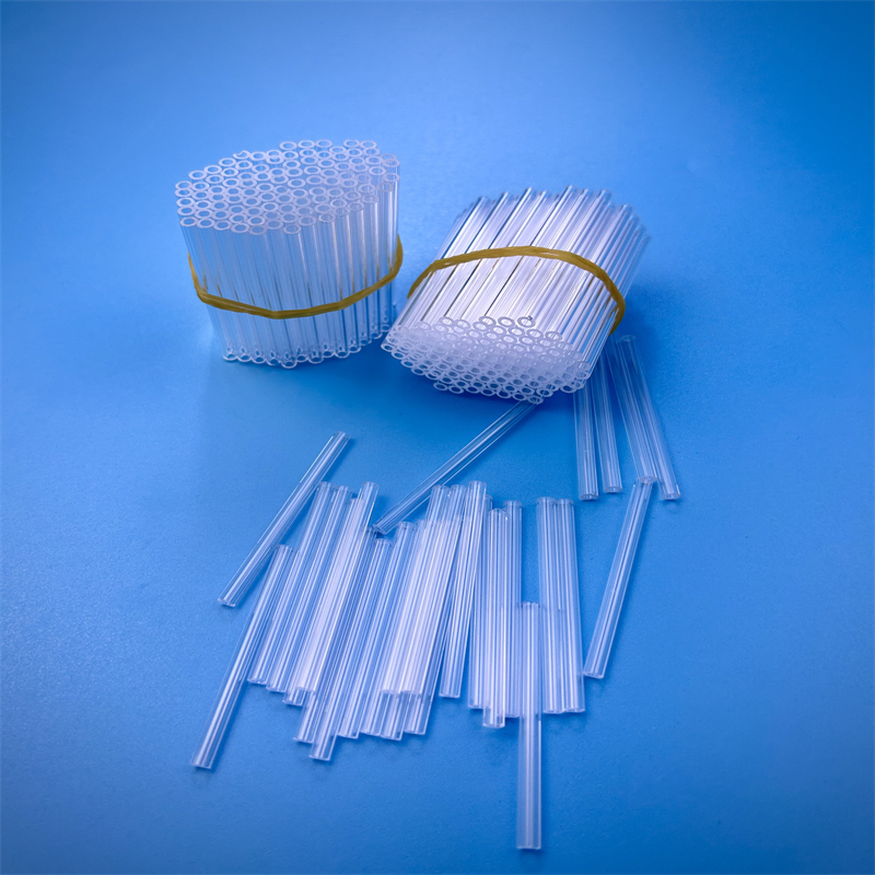
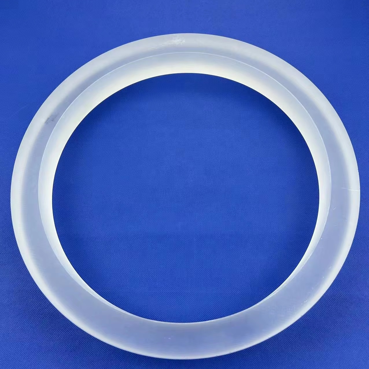
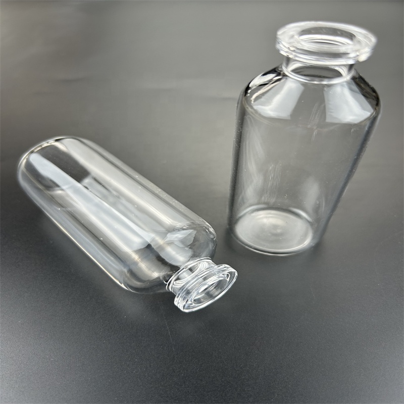

The Espoo Deep-Tech Landscape: Elevating Quartz Substrate Demands
The innovation corridor spanning Otaniemi, Keilaniemi, and the broader Espoo municipal region in Finland represents one of Northern Europe’s dense microelectronics, nanophotonics, and quantum engineering clusters. Anchored by world-renowned institutions such as VTT Technical Research Centre of Finland, Aalto University Micronova cleanroom facilities, and leading commercial innovators in superconducting quantum processors, the requirements for optical-grade fused silica (JGS1) and thermal quartzware have evolved significantly.
Unlike commodity glass products, quartz substrates procured by Finnish deep-tech organizations serve under stringent environmental metrics: cryogenic interfaces within dilution refrigerators, ultra-clean carrier wafers inside metal-organic chemical vapour deposition (MOCVD) systems, and deep-UV optical transmission windows for sub-micron inspection rigs. In these environments, material micro-inhomogeneities, trace bubble clusters, or dielectric losses lead directly to coherence degradation or lithographic wavefront aberrations.
Information Gain Insight: Modern quantum and photonic fabs in Espoo require high electrical resistivity (>1018 Ω·cm at room temperature), ultra-low loss tangent (<0.0001 at 10 GHz), and minimal hydroxyl (−OH) absorption peaks at 2.73 μm (specifically via JGS3 IR-grade quartz), paired with localized edge chamfering that eliminates micro-chipping during automated silicon-substrate bonding.
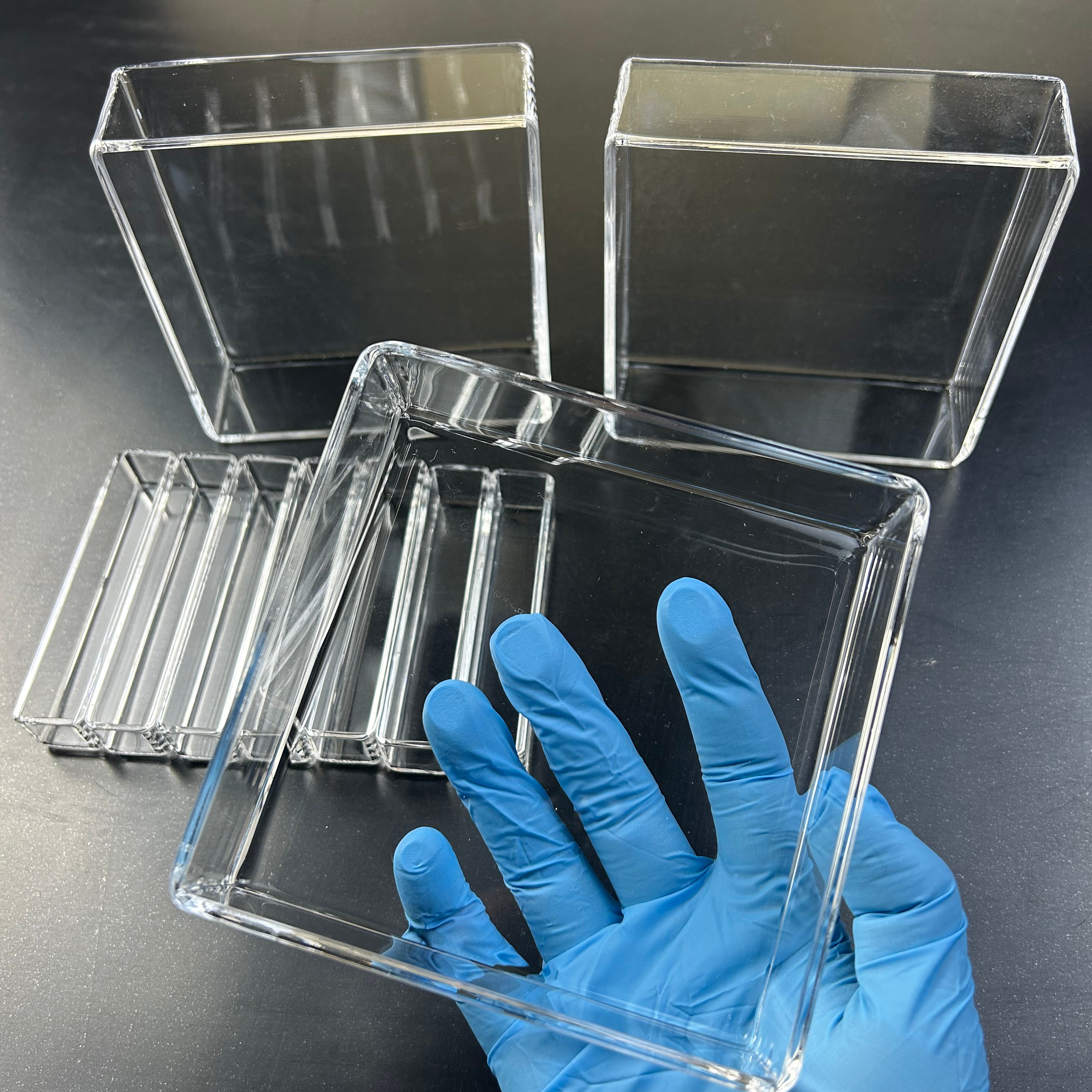
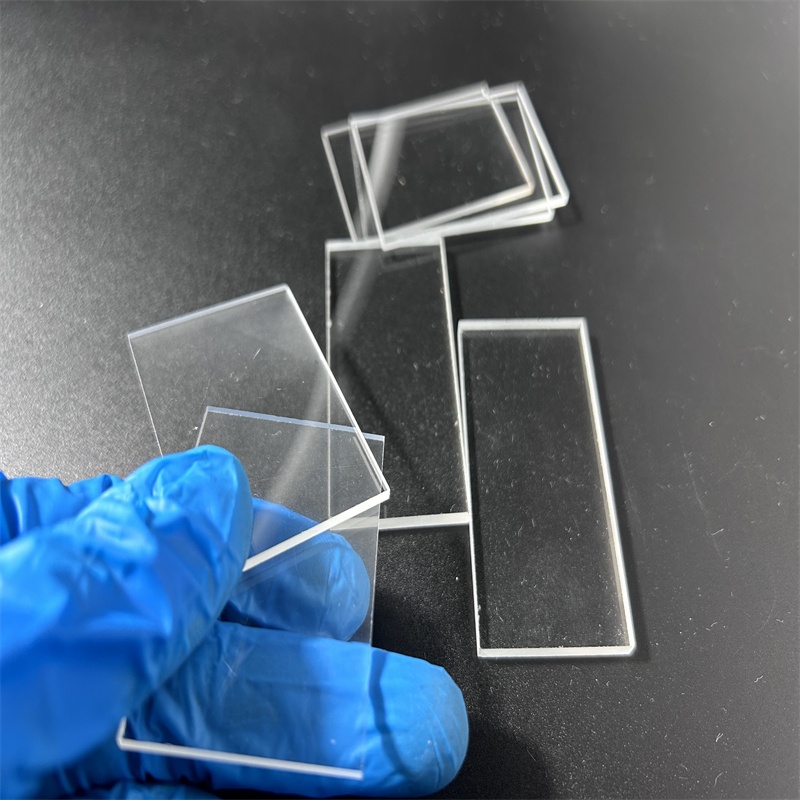
As an OEM/ODM direct manufacturer based in Donghai County—the crystal and silicon capital of China—Zunex Quartz Products Co., Ltd. fills a vital supply chain link. We deliver high-specification bespoke fused silica substrates, XRD specimen plates, and multi-slotted wafer boats directly from primary material synthesis to Espoo’s high-tech manufacturing floors, eliminating multi-tier brokerage markups and engineering misalignments.
Targeted Integration
Localized Industrial Applications Across the Uusimaa Region
Engineered to match the exact experimental and series production setups found across Espoo’s technology hubs.
Quantum Circuit Carriers & Cryo-Packaging
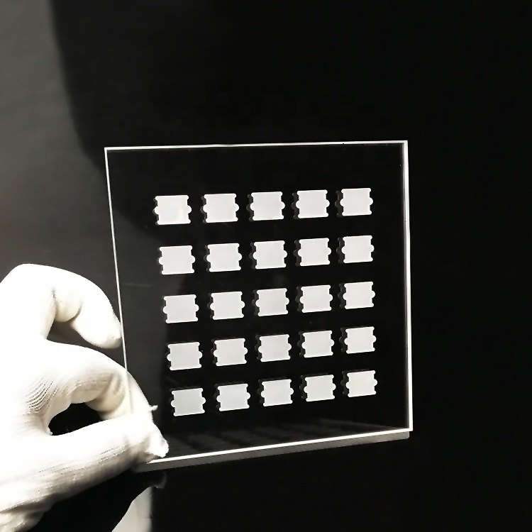
Ultra-low dielectric loss JGS1 substrates providing high microwave isolation for superconducting transmon qubits. Polished down to Ra < 0.5 nm, ensuring flat deposition surfaces for superconducting niobium, aluminium, or titanium-nitride thin films.
Cleanroom CVD & ALD Consumables
Engineered for Micronova-grade atomic layer deposition (ALD) and chemical vapor deposition apparatus. Flanged U-bent process tubes, furnace quartz liners, and slotted carriers capable of surviving continuous thermal cycling at 1100 °C without devitrification.
Integrated Photonics & DUV Sensors
Optically isotropic fused silica wafers with internal transmission exceeding 90% at 193 nm. Ideal for high-density optical waveguide manufacturing, biosensor interposer layers, and laser excitation apertures designed for precision spectroscopic sensing.
XRD & Material Analysis Tanks
X-ray diffraction zero-background plates and slotted testing carriers crafted from selected amorphous fused quartz, delivering zero peak interference during structural crystal characterization in mineral, polymer, and battery anode research.
Pulsed Laser & IR Optics Platforms
JGS3 low-OH content components engineered for high-power infrared fiber laser systems and gas sensors, guaranteeing absence of characteristic absorption dips in the 2.6 μm to 2.8 μm spectrum, avoiding optical runaway.
Biotech Microfluidic Substrates
Laser-drilled and grooved quartz bases facilitating high chemical inertness against concentrated acids, organic solvents, and enzymatic reagents, enabling high-resolution fluorescence monitoring in next-generation gene analysis.
Market Trends: Why Northern Europe’s Hardware Shift Favors Custom Quartz ODM
Finland’s ambitious strategic roadmap—backed by Business Finland, the European Chips Act, and domestic venture initiatives—is rapidly expanding localized wafer fab capacity and pilot lines. Several systemic procurement trends are shaping how purchasing officers and principal investigators in Espoo source non-standard quartz consumables:
1. Transition from Standard Catalog to Iterative Rapid Prototyping
Traditional catalog distributors often impose prohibitive lead times (12–18 weeks) and rigid MOQ constraints for customized round, square, or slotted quartz substrates. Finnish R&D groups run iterative development sprints demanding fast CAD-to-part production cycles where dimensional tolerances (down to ±0.02 mm) and notch geometries change between test lots.
2. Stringent Impurity Traceability for Cleanroom Qualification
Trace transition metal contamination (Fe, Cu, Ni) at levels above 1.0 ppm can ruin semiconductor diffusion furnaces and cause parasitic charge traps in quantum dot architectures. Nordic hardware manufacturers actively shift away from secondary traders towards vertically integrated manufacturers capable of providing ICP-MS batch analysis.
3. High-Precision Laser Micro-Drilling vs. Mechanical Tooling
Mechanical drilling of brittle quartz plate inevitably leaves subsurface micro-fractures, which expand under 1100 °C thermal cycles or vacuum stresses. Modern Finnish integration standards require non-contact CO₂ and picosecond laser drilling and groove cutting to yield edge quality with micro-crack limits strictly under 15 μm.
4. Total Landed Cost Rationalization Amid Escalating European R&D Costs
Securing direct-from-factory pricing from the premier raw materials cluster in Donghai affords Espoo-based commercial enterprises and universities savings up to 45% compared to Western European intermediaries, while maintaining identical or superior physical properties.
Empirical Data Verification
Material Grade Comparison & Physical Specifications
Select the optimal synthetic fused silica or natural fused quartz grade based on spectral transmission and thermal envelope parameters.
| Characteristic / Parameter | JGS1 (Synthetic Fused Silica) | JGS2 (Optical Grade Quartz) | JGS3 (Infrared Grade Quartz) |
|---|---|---|---|
| Primary Optical Transmission Band | 185 nm – 2500 nm (Deep UV to NIR) | 220 nm – 2500 nm (Standard UV-Vis) | 260 nm – 3500 nm (Extended IR) |
| Hydroxyl Content (OH−) | ≤ 1200 ppm (Typical) | ≤ 150 – 200 ppm | ≤ 5 – 10 ppm (Water-free) |
| SiO₂ Purity (Trace metals excluded) | ≥ 99.999% | ≥ 99.99% | ≥ 99.98% |
| Continuous Working Temperature | 1100 °C | 1100 °C | 1150 °C |
| Short-term Maximum Temperature | 1300 °C | 1300 °C | 1350 °C |
| Thermal Expansion Coeff. (20–320 °C) | 5.5 × 10⁻⁷ / °C | 5.5 × 10⁻⁷ / °C | 5.4 × 10⁻⁷ / °C |
| Surface Flatness / Roughness (Available) | λ/4, Ra < 0.5 nm (Super-polished) | λ/2, Ra < 1.0 nm | Commercial polish, Ra < 2.0 nm |
| Key Regional Application in Espoo | Quantum gates, UV photolithography | Sight windows, process viewports | IR laser windows, high-temp sensors |
The Zunex Manufacturing Edge
Engineered in China's Crystal Capital for Global Tech Leaders
Combining Donghai’s raw material reserves with ISO-certified micro-machining and dedicated B2B international logistics.
Donghai Raw Material Origin
Located directly in Donghai County, Jiangsu, giving us direct access to high-purity natural silica sand (≥ 99.99%) and synthetic feedstock. This vertical foundation minimizes raw material lead times and insulates clients from global supply spikes.
Laser Micro-Finishing Specialty
In-house advanced multi-axis laser machining setups for non-contact cutting, drilling, and micro-grooving. Achieve diameter apertures down to 0.2 mm with minimal thermal taper, ultra-clean bevels, and smooth surface edge transitions.
Rigorous Defect & Cleanliness Control
Every batch undergo precision interferometry inspection, ultrasonic solvent cleaning, polarized strain verification, and bubble inclusion screening conforming to DIN ISO 10110 optical standards prior to certified vacuum sealing.
Direct Engineer-to-Buyer Review
Your technical inquiry is evaluated immediately by senior optical and glass engineers. Within ≤ 2 hours, we verify STEP, DWG, or PDF design tolerances, thermal expansion parameters, and material machinability before final quotation.
Prototyping to High-Mix Batch Scale
Whether an academic research project at Aalto University requires 5 bespoke XRD holders or an industrial scaleup in Otaniemi schedules thousands of quarterly substrate units, our modular capacity guarantees flexible scheduling and consistency.
Zero-Breakage Nordic Export Packaging
Decades of worldwide air-freight experience delivering fragile quartzware into Scandinavia. Multi-layer shock-absorbent poly-foam, vacuum-sealed electrostatic wrapping, and ISPM-15 compliant plywood crating guarantee damage-free delivery.
Procurement Clarity
Frequently Asked Questions for Espoo Importers
Addressing core technical tolerances, logistics timelines, import compliance, and customized prototyping protocols.
What specific geometric tolerances and surface roughness can Zunex deliver on quartz substrates?
For precision OEM quartz substrates, our standard CNC milling achieves linear tolerances of ±0.05 mm, with high-precision double-sided lapping and polishing delivering dimensional accuracy down to ±0.01 mm and thickness tolerances within ±0.005 mm. Standard optical surfaces achieve 60/40 scratch/dig, while specialized synthetic fused silica wafers for lithography or quantum thin-film deposition can be finished to 20/10 or 10/5 scratch/dig with surface roughness Ra < 0.5 nm (< 5 Å).
How do you handle shipping to Espoo (Finland) and ensure fragile components arrive without damage?
Shipments dispatched to Helsinki-Vantaa Airport (HEL) and onward to Espoo are routed via DHL Express, FedEx, or dedicated air-freight forwarders, with typical transit durations ranging from 4 to 7 business days. Products are individually cleanroom-dusted, vacuum-sealed in anti-static PE bags to prevent environmental moisture or particulate adhesion, cocooned within high-density expanded polyethylene (EPE) shock cells, and boxed into heavy-duty reinforced corrugated master cartons or customized export plywood crates with integrated tilt and shock indicators.
Which quartz grade should we choose between JGS1, JGS2, and JGS3 for quantum and optical sensors?
Select JGS1 if your application operates in the deep ultraviolet spectrum (185–250 nm), requires near-zero bubble classification, or functions as a carrier substrate for low-loss microwave qubits where synthetic purity minimizes parasitic dielectric attenuation. Select JGS2 for general optical sight windows, analytical cuvettes, and standard ultraviolet/visible inspection instrumentation. Choose JGS3 if your optical components operate in the infrared spectrum up to 3.5 μm, as JGS3 is chemically synthesized to eliminate the characteristic −OH absorption band at 2730 nm.
Can we submit confidential STEP or DWG drawings, and do you support prototyping batches?
Yes. We routinely execute mutual Non-Disclosure Agreements (NDAs) with European university labs, tech enterprises, and defense contractors prior to drawing exchange. We welcome low-volume pilot prototype runs (from 2 to 10 units) to validate fit, vacuum performance, and thermal resilience prior to series production. CAD drawings in 3D STEP/IGES or 2D DWG/DXF/PDF formats are reviewed directly by our engineering department within 2 hours.
What compliance documentation accompanies our export consignment?
Every export consignment shipped to the European Union is accompanied by a Certificate of Conformance (CoC), material spectral transmission charts upon request, dimensional inspection reports, and full compliance declarations conforming to EU RoHS (Directive 2011/65/EU) and REACH (EC 1907/2006) regulations, verifying the total absence of restricted hazardous substances.
How resistant are your fused quartz crucibles and tubes to rapid thermal shock?
Because high-purity fused silica exhibits an exceptionally low linear coefficient of thermal expansion (α ≈ 5.5 × 10⁻⁷ / °C), our quartz tubes, circular crucibles, and XRD tanks can withstand severe thermal shock. A typical component heated to 1100 °C can be plunged into cold water without experiencing catastrophic mechanical fracturing. Continuous operating exposure is rated up to 1100 °C, with short excursions reaching 1300 °C.
Have a Custom Drawing or Technical Specification?
Direct factory engineering review · Transparent ODM/OEM pricing · Rapid air delivery to Espoo and across the Nordic region.
Get a Quote