Featured Semiconductor & Optical Quartzware
Manufactured to micron-level mechanical tolerances with deep-ultraviolet (DUV) through mid-infrared (MIR) transmission characteristics, certified for cleanroom wafer processing and advanced photonics.
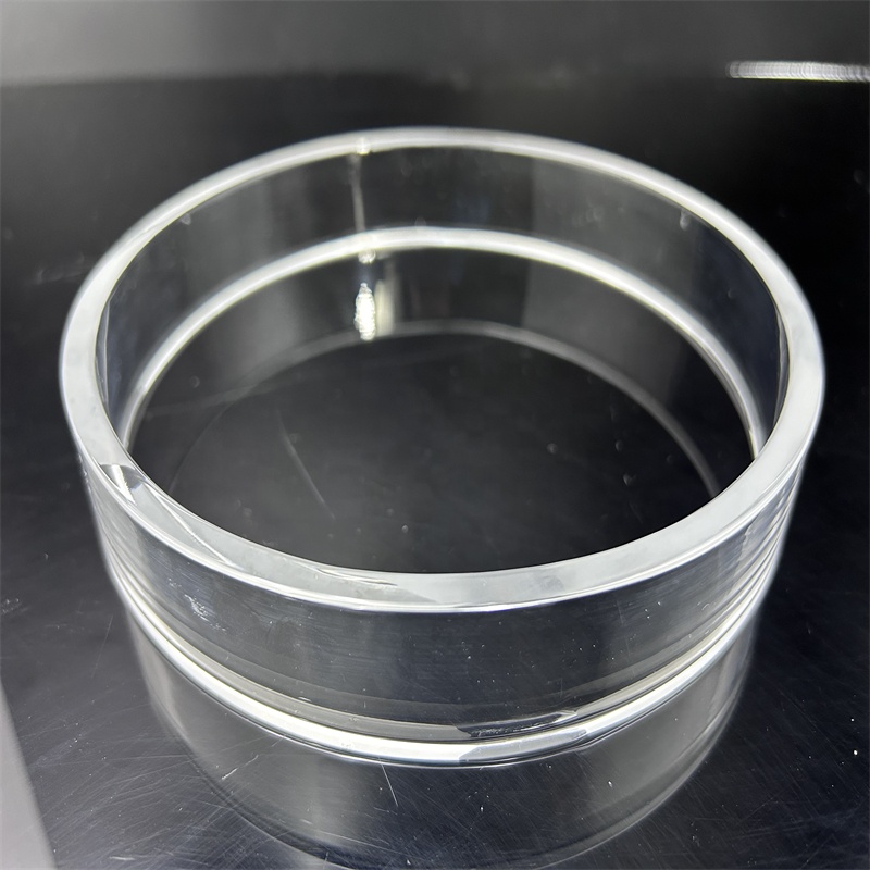
High-Purity Fused Quartz Bell Jar for Semiconductor Deposition
Heavy-wall fused quartz vacuum chambers engineered for high-temperature CVD, plasma etching, and epitaxial silicon growth with low devitrification.
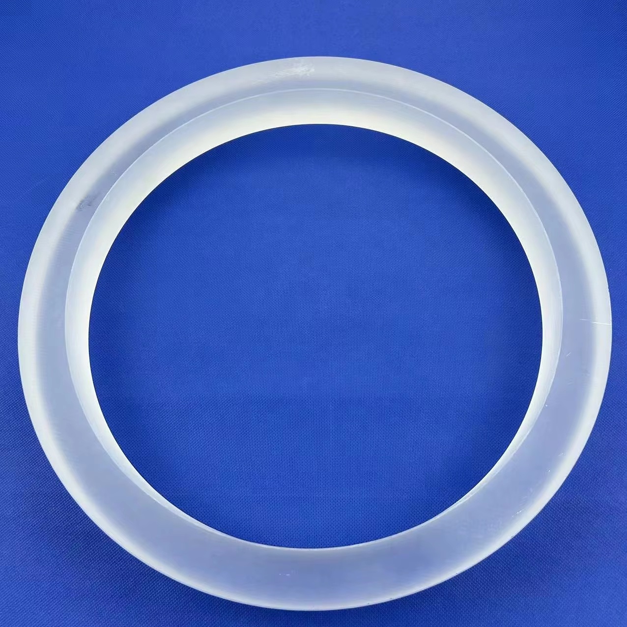
Custom High-Purity Quartz Rings for CVD & Optics Assembly
Ultra-low tolerance retaining, clamp, and plasma shielding rings crafted from semiconductor-grade fused quartz with optional dielectric anti-reflective thin films.
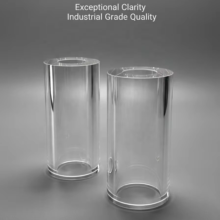
Polished Transparent Quartz Twin Tube (Dual-Bore Fabrication)
Precision dual-bore quartz tube profiles for advanced halogen IR thermal processing, directional heating filaments, and uniform wafer curing.
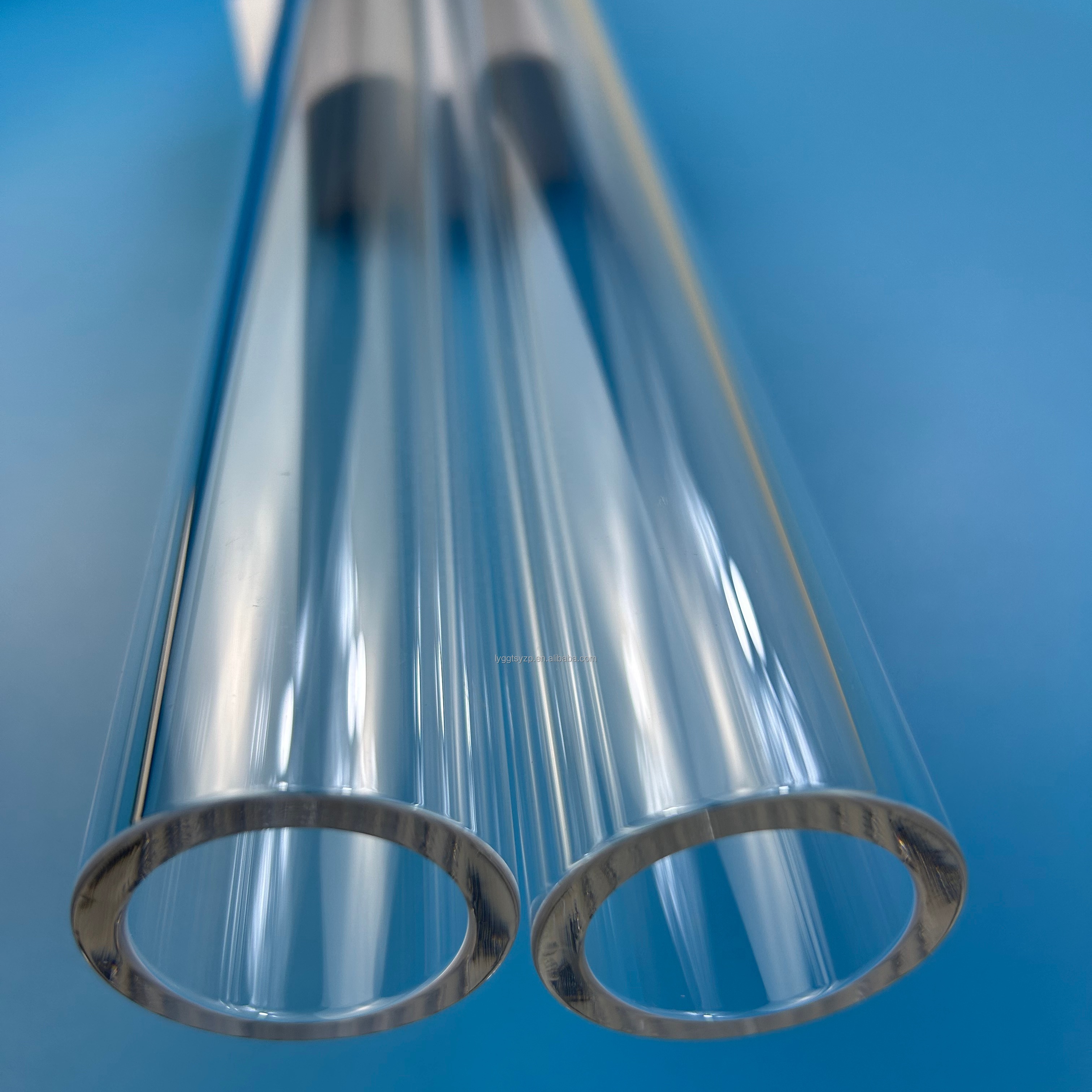
Clear Ozone-Free Quartz Twin Tube for Furnace Heaters
Specialized doped fused silica that cuts 185nm ozone-forming UV radiation while delivering optimal 254nm UV and high infrared thermal energy transfer.
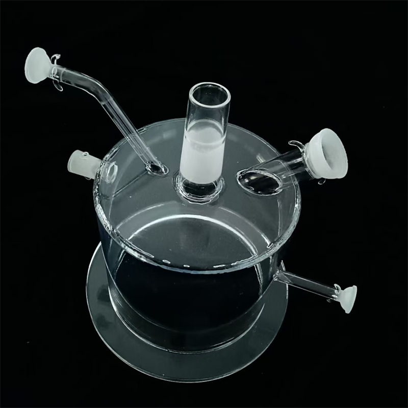
High-Pressure Clear Quartz Process Tubes (Custom Bent & Flanged)
Heavy-wall fused silica glass tubing engineered for aggressive thermal shock resistance, oxidation tubes, gas injectors, and chemical reactor conduits.
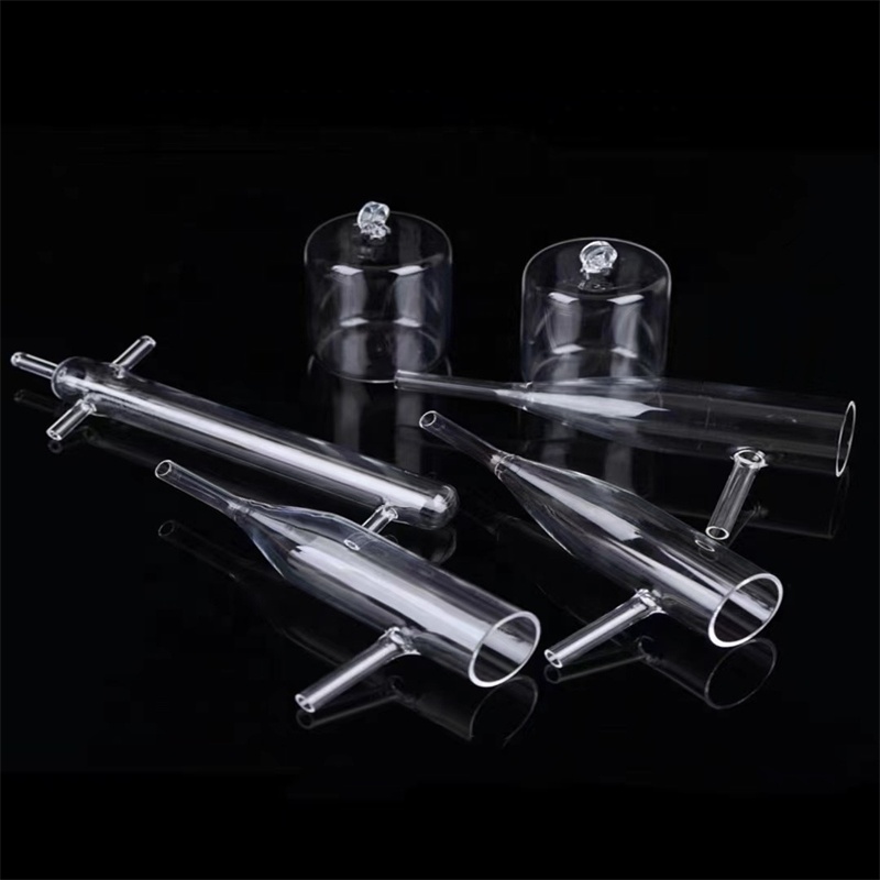
Laboratory High-Temperature CVD Furnace Quartz Twin Tube
Precision flame-worked vacuum twin glass vessels for scientific R&D, graphene syntheses, and chemical vapor deposition furnace lines.
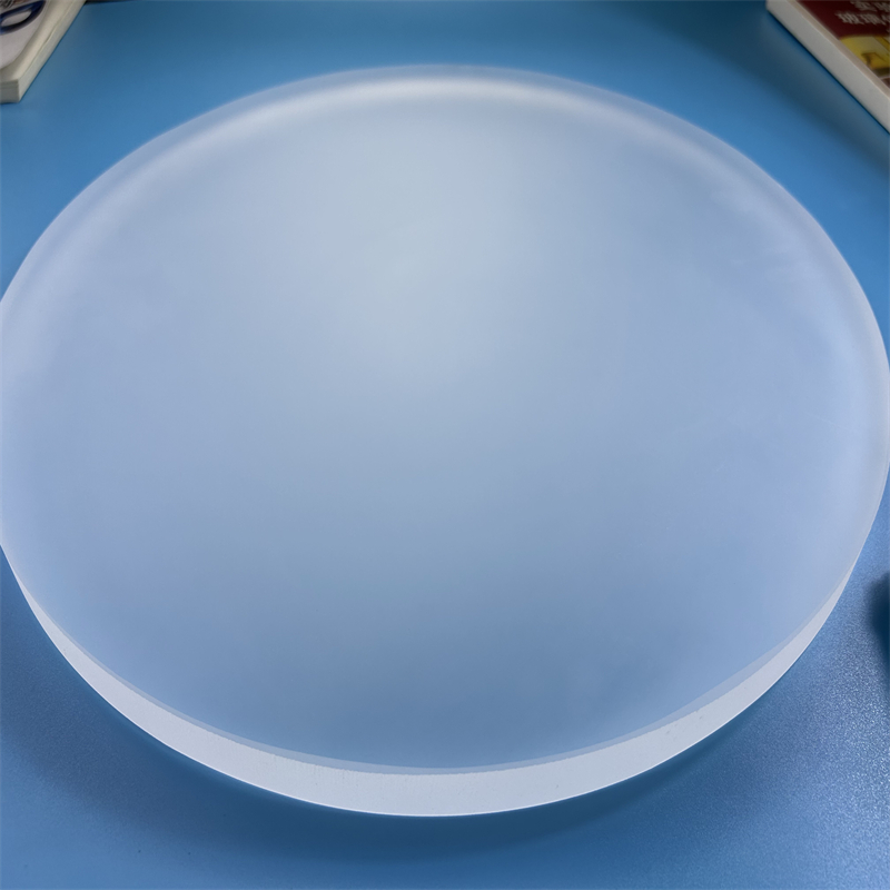
High-Temperature Frosted Fused Quartz Disc & Baffle Plates
Surface-conditioned matte and frosted quartz baffle plates used for thermal radiation homogenization, heat shields, and furnace zone isolation.
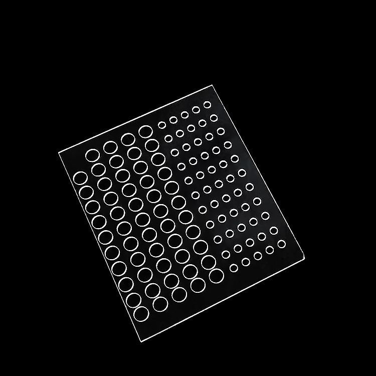
Optical Grade Fused Quartz Plates & Windows (0.5mm – 100mm)
Ultra-flat double-side polished optical windows with scratch-dig 20/10 surface quality, engineered for laser viewports, lithography masks, and sensors.
Optical Grade Fused Silica vs. Fused Quartz: Selection Criteria for Cleanroom & Photonic Applications
In high-reliability manufacturing ecosystems like Singapore’s semiconductor fabrication plants (fabs) and precision optical R&D laboratories, choosing between synthetic fused silica and natural fused quartz directly determines component lifetime, thermal drift, and optical transmission efficiency. While both materials boast a chemical formulation dominated by silicon dioxide (SiO₂), their manufacturing origins dictate vastly distinct spectral performance curves, trace metallic impurity thresholds, and hydroxyl (OH⁻) content.
Optical Grade Spectral Differentiation: JGS1 vs. JGS2 vs. JGS3
Optical design engineers and procurement teams across Singapore must carefully categorize quartz substrate grades based on the operational spectral transmission band required:
| Optical Grade | Equivalent Standard | Transmission Band | Hydroxyl (OH⁻) Content | Primary Singapore Industrial Applications |
|---|---|---|---|---|
| JGS1 (Synthetic Fused Silica) | Suprasil 1/2, Corning 7980 | 185 nm – 2,500 nm (Deep UV) | Typical: 800 – 1,200 ppm | DUV Photolithography steppers, excimer laser windows (193nm/248nm), silicon photonics coupling waveguides. |
| JGS2 (Optical Fused Quartz) | Homosil, GE 124 / 214 | 220 nm – 2,500 nm (UV-Vis) | Typical: < 30 ppm | Semiconductor inspection viewport sight glasses, UV curing lamps, etching chamber viewing ports, wafer pyrometry. |
| JGS3 (Infrared Fused Quartz) | Infrasil 301/302, Electrically Fused | 260 nm – 3,500 nm (IR-Extended) | Ultra-low: < 5 ppm | High-temperature FTIR spectroscopy, IR heating elements, defense thermal imaging, laser cutting optics. |
Trace Metallic Contamination Limits in Semiconductor Fabrication
For front-end wafer fabrication facilities in Woodlands and Tampines, metallic ion leaching under elevated thermal loads represents a catastrophic risk for CMOS transistor gate oxides. Sodium (Na), Potassium (K), Iron (Fe), and Copper (Cu) act as deep-level recombination centers, drastically degrading electron carrier lifetimes. Our high-purity synthetic fused quartz maintains total metallic impurity levels below 1.0 ppm (with typical alkaline elements Na < 0.05 ppm, K < 0.05 ppm, and Li < 0.02 ppm), verified via Inductively Coupled Plasma Mass Spectrometry (ICP-MS).
Thermal Shock Tolerance
Extremely low coefficient of thermal expansion (CTE: 5.5 × 10⁻⁷ /°C from 20°C to 320°C). Quartzware can survive instantaneous quenching from 1100°C into ice water without mechanical failure.
Micro-Laser Processing
Using cold UV picosecond laser trepanning, we fabricate micro-apertures down to 0.1 mm diameter with edge chipping < 15 μm, avoiding micro-cracks inherent to traditional diamond drilling.
Surface Finish & Flatness
Optically polished plates feature surface roughness Ra < 0.5 nm, scratch-dig 20/10 or 10/5 per MIL-PRF-13830B, and transmitted wavefront distortion < λ/10 at 632.8 nm.
Localized Application Scenarios in Singapore
Singapore represents one of the world's most dense concentrations of high-tech manufacturing, accounting for approximately 11% of the global semiconductor market and 20% of precision semiconductor equipment manufacturing.
Front-End Wafer Fabs (Woodlands & Tampines)
Critical consumable quartzware deployed in diffusion furnaces, LPCVD chambers, and wet etch benches across Micron, GlobalFoundries, SSMC, and Siltronic lines. Items include 200mm/300mm wafer carriers, furnace process tubes, thermocouple protective sheaths, and exhaust gas scrubbers.
Silicon Photonics & A*STAR R&D Hubs
Substrates and optical windows for advanced photonics research at Fusionopolis, Biopolis, and A*STAR Institute of Microelectronics (IME). JGS1 optical quartz flats are utilized for laser beam steering, multi-channel waveguide packaging, and cryogenic optical measurement cavities.
Biomedical Diagnostics & Tuas Life Sciences
Singapore's pharmaceutical and life-sciences manufacturing corridor in Tuas relies heavily on our chemically inert quartz cuvettes, UV-transmissive flow cells, and spectrometry cells for real-time online spectroscopy, analytical chromatography, and vaccine purity inspection.
Precision Aerospace & Seletar Sensor Optics
Aviation and defense clusters at Seletar Aerospace Park implement high-temperature fused quartz pressure windows, pyrometry sight glasses, and flight sensor enclosures capable of withstanding extreme aerodynamic friction and sudden stratospheric thermal variations.
Trends Shaping Quartz Procurement Under Singapore RIE2025
Singapore's Research, Innovation and Enterprise (RIE2025) Plan continues to pump substantial investment into advanced manufacturing, sub-nanometer semiconductor packaging, and decarbonization.
Heterogeneous 2.5D/3D Chiplet Packaging
With Singapore becoming an epicenter for advanced packaging, quartz substrates are displacing conventional borosilicate carriers. High dimensional stability, low dielectric loss, and thermal expansion matching silicon make fused silica wafers (100mm to 300mm) the gold standard for temporary bonding and wafer thinning carriers.
Cleanroom Thermal Decarbonization
Local fabs are actively phasing out high-loss resistive furnace coils in favor of rapid thermal processing (RTP) powered by specialized twin-tube clear quartz infrared emitters. These systems deliver targeted thermal profiles with instantaneous warm-up/cool-down cycles, cutting fab energy footprints by up to 28%.
Supply Chain Regionalization & Dual-Sourcing
Recent global supply chain disruptions have driven Singapore procurement directors to bypass extended European lead times (frequently exceeding 26–36 weeks) in favor of verified direct manufacturers in Asia capable of delivering OEM-equivalent drawing custom fabrication within 3–4 weeks.
Why Singapore Engineers & Buyers Partner With Us
Headquartered with direct production in Donghai County—the world-renowned capital of quartz crystal refining—Zunex Quartz combines primary mineral supply advantages with ultra-precise CNC and laser fabrication technologies.
Direct Source Advantage
Integrated processing directly from raw high-purity natural quartz sand and synthetic precursor gases. Zero intermediary markup, guaranteed lot-to-lot chemical consistency, and verifiable raw material origin certificates.
Precision Laser Finishing
Our facility houses 5-axis CNC machining centers, precision glass-blowing lathes, and state-of-the-art laser cutting/drilling units capable of producing tight tolerances within ±0.005 mm on optical plates and flanged tubes.
Stringent Metrology & Clean Packaging
Every shipment bound for Singapore is inspected using laser interferometers, surface profilometers, and spectrophotometers. Parts receive ultrasonic high-purity DI water cleaning and are vacuum sealed in Class 100/1000 cleanroom packaging.
Accelerated Logistics to Singapore
Leveraging strategic air links from Shanghai/Lianyungang to Singapore Changi Airport (SIN), standard custom prototypes arrive at your facility in Singapore within 5–7 business days post-machining, fully cleared for GST import.
Singapore Buyer FAQ: Custom Quartzware & Optical Sourcing
Detailed answers addressing engineering parameters, cleanroom packaging, GST regulations, and logistics protocols for Singapore-based purchasing teams.
How are import tariffs and Singapore GST handled for quartzware consignments?
What cleanroom cleaning and packaging protocols are implemented before shipment to Singapore?
Can you manufacture replacement quartz components from existing OEM tool part numbers?
What is the typical lead time for custom prototype vs. volume production orders shipped to Singapore?
What technical documentation and material certifications accompany each consignment?
How does your pricing compare with local Singapore quartz fabricators or European distributors?
Need Custom Quartzware Machined to Your Exact Drawing?
Send your PDF, DWG, or STEP files along with your required purity grade (JGS1/JGS2/JGS3) and quantity. Our optical and semiconductor fabrication engineers will review manufacturability, verify tolerances, and deliver a formal quotation within 2 hours.