High-Purity Quartzware & Optical Transmission Components
Direct OEM manufacturing to micron-level tolerance. Featuring fully fused, acid-welded, and flame-polished fused silica engineered for spectrophotometry, semiconductor CVD, and critical photonic analysis.
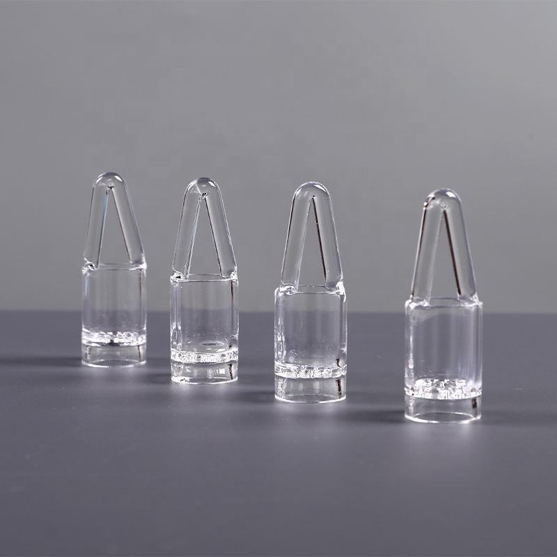
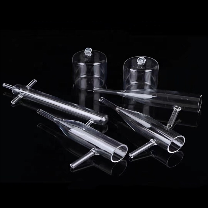
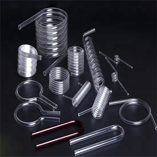
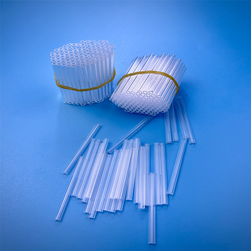
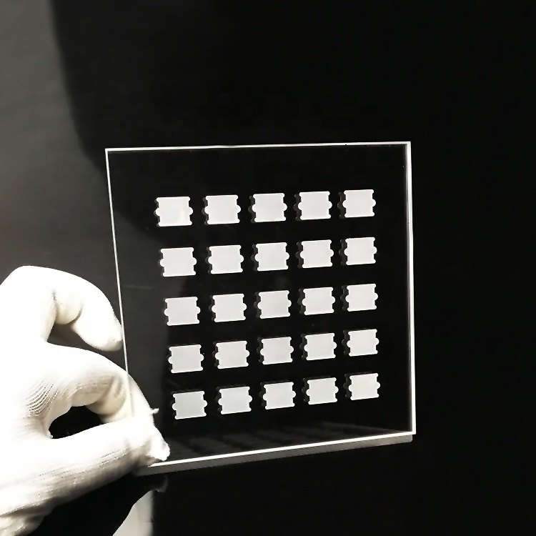
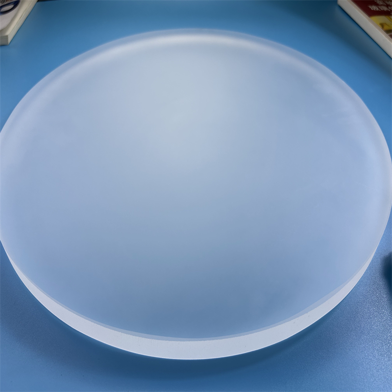
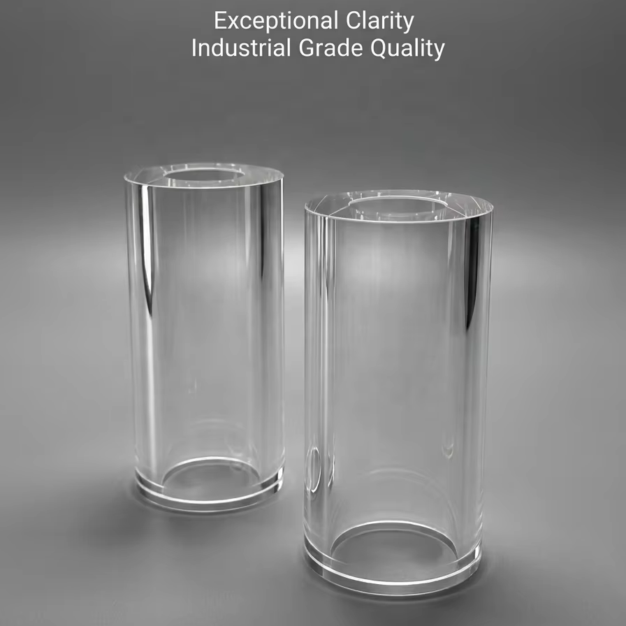
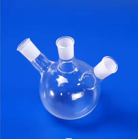
Sub-Nanometer Optical Physics in Modern Spectroscopy
UV quartz cuvettes utilized across the Santa Clara and Silicon Valley semiconductor corridors are subjected to rigorous photolithographic and chromatographic inspection. Standard borosilicate glass exhibits extreme solarization and opaque transmission cutoff below 320 nm, making quantitative UV-Vis spectroscopy, DNA/RNA quantification at 260/280 nm, and chemical mechanical planarization (CMP) slurry characterization completely unfeasible.
By implementing thermal fusion of JGS1 synthetic fused silica (derived from high-temperature chemical vapor deposition of silicon tetrachloride), our optical cells eliminate trace transition metal contaminants (Fe, Cu, Ni < 0.1 ppm). This guarantees zero secondary fluorescence, complete resistance to aggressive solvolysis, and uncompromising transmission integrity down to 185 nm in deep ultraviolet applications.
Fused Silica Optical Performance Benchmarks
Comparative metallurgical & optical data based on certified standard testing (DIN ISO 3585).
| Physical / Optical Property | Standard UV Quartz (JGS1) | Optical Fused Quartz (JGS2) |
|---|---|---|
| UV Spectral Cutoff Range | 185 nm – 2500 nm | 220 nm – 2500 nm |
| Transmittance @ 200 nm (10mm path) | > 90.5% (Certified) | < 70.0% |
| Hydroxyl Content [OH⁻] | < 5 ppm to < 20 ppm | 150 ppm – 300 ppm |
| Coefficient of Thermal Expansion | 5.5 × 10⁻⁷ / °C | 5.5 × 10⁻⁷ / °C |
| Annealing Point / Max Strain Point | 1215 °C / 1120 °C | 1200 °C / 1100 °C |
| Internal Window Parallelism | < 15 arcseconds | < 30 arcseconds |
High-Precision Applications in the Santa Clara Ecosystem
Serving cleanrooms, fab instrumentation teams, biopharmaceutical hubs, and photonics research laboratories from Great America Parkway to Silicon Valley Boulevard.
Wafer Fab Wet Bench Metrology
Critical in-line concentration monitoring of SC-1, SC-2, and piranha etch baths in cleanroom automated chemical supply units across Santa Clara fabs.
- Eliminates metallic contamination (Fe, Na, K < 5 ppb)
- Hydrofluoric (HF) chemical compatibility flow-cells
- Zero beam dispersion on 193 nm / 248 nm photometers
CMP Slurry Characterization
Specialized micro-cuvettes and double-ended flow cells configured to avoid dynamic particle adhesion during chemical mechanical planarization analysis.
- Laser diffraction particle sizing without window scratch
- Optically polished side-walls (80/50 Scratch-Dig)
- Resistance to abrasive colloidal silica suspensions
Biopharma & Gene Sequencing
Ultra-micro UV cuvettes designed for protein concentration, genomic fluorometry, and high-performance liquid chromatography (HPLC) detection units.
- Path length tolerance maintained down to ±0.005 mm
- Sample volumes as low as 10 microliters (µL)
- Non-fluorescent under deep 254 nm UV excitation
Silicon Valley Academic & R&D Centers
Supplying institutional R&D entities, contract research organizations (CROs), and incubation laboratories across Northern California.
- Customized XRD quartz sample holders with zero background
- High vacuum CVD furnace double-wall reaction tubes
- Rapid CAD-to-glass prototyping for grant projects
Emerging Trends in Santa Clara’s Photonic & Fab Supply Chain
Understanding shifting technical mandates and how local procurement heads optimize optical component acquisition.
Shift to Sub-3nm Metrology Demands
As semiconductor process nodes shrink below 3nm across advanced Bay Area test facilities, inline chemical analytical systems require optical transmission stability with lower absorbance noise (< 0.0001 AU). Standard glass and multi-piece bonded cells fail under aggressive laser exposure. Santa Clara engineering teams increasingly mandate single-piece, flame-fused JGS1 quartz components that resist thermal optical distortion and avoid polymer outgassing.
Domestic Inventory + Direct OEM Agility
Supply chain security has evolved into a strategic priority for Santa Clara fab managers. Rather than relying on multi-tier local distributors with inflated lead times, procurement specialists are forging direct factory connections with manufacturers capable of custom laser machining (grooving, micro-apertures, flanging) while maintaining pre-inspected inventory ready for expedited air transit directly into SFO and San Jose international hubs.
Transition to Automated Continuous Flow
Traditional static cuvettes are rapidly giving way to customized quartz flow-through cells in bio-manufacturing and automated semiconductor wafer-cleaning stations. Facilities near Santa Clara require seamless integration of barbed quartz fittings, precision micro-bore twin tubes, and laser-drilled sampling ports that withstand continuous corrosive chemical circulation at temperatures exceeding 250°C.
Why Silicon Valley Procures from Zunex Quartz
Operating from China’s quartz crystal capital with complete vertically integrated laser finishing and verified export transparency.
Advanced Laser Finishing
Proprietary quartz laser drilling, precise slotting, micro-grooving, and burr-free optical slicing down to ±0.01 mm without inducing micro-fractures in the quartz substrate.
≤ 2h Engineering Turnaround
Our 100% verified response rate ensures that CAD drawings (DWG, STEP, PDF) sent by Silicon Valley design engineers are evaluated for manufacturability within two hours.
100% Thermal Fusion Integrity
All UV cuvettes and multi-chamber quartzware are fused entirely by precision flame or molecular fusion without adhesive glues, ensuring absolute resistance to acids, bases, and organic solvents.
Verified Trade Performance
Documented 43% repeat-order rate from international industrial buyers, backed by accredited third-party Alibaba audit reports, ISO-compliant quality inspections, and zero-defect protective packaging.
Frequently Asked Questions by Santa Clara Buyers
Essential technical clarifications regarding custom path lengths, UV material grades, cleanroom packaging, and delivery timelines.
What makes JGS1 fused silica superior to standard optical glass in Santa Clara lab applications?
Are your UV quartz cuvettes adhesive-free and capable of withstanding corrosive solvents?
Can you produce custom optical path lengths and micro-volume flow cells to engineering drawings?
How do you protect fragile optical quartzware during transit to the California Bay Area?
What are the thermal shock limitations of your CVD furnace tubes and quartz flasks?
Need instant specifications, pricing confirmation, or factory material certificates?
Get a Quote