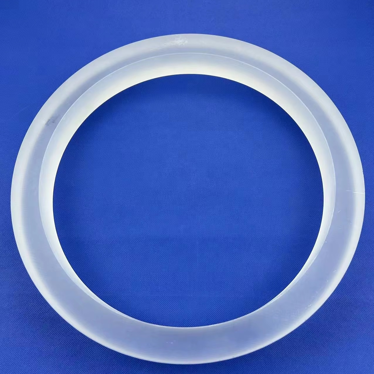
 Semiconductor CVD
Custom Coated 99.99% Pure Quartz Rings for Semiconductor CVD Optics Applications High Pressure Moulding/Bending/Welding/Cutting
- Purity: ≥ 99.99% SiO2
- Tolerance: ±0.02 mm CNC
- Surface: Optical Polish / Custom Coating
Fabricated from raw crystal sands in Donghai County with purity exceeding 99.99% SiO2. Each component undergoes strict thermal annealing, multi-axis CNC shaping, laser micro-drilling, and full spectral photometric validation.
Semiconductor CVD
 Thermal Radiation
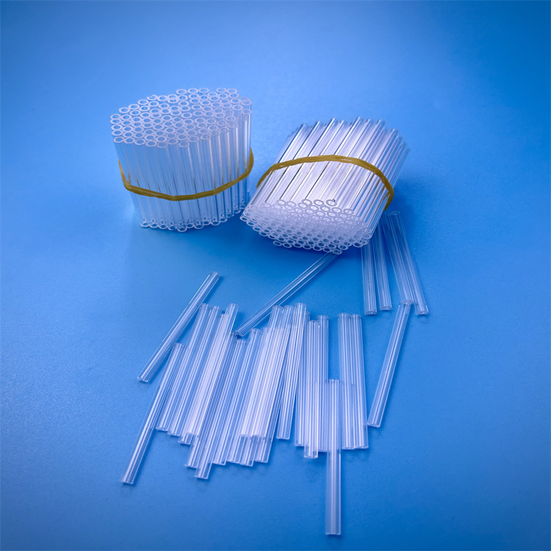 Custom Hot Forming
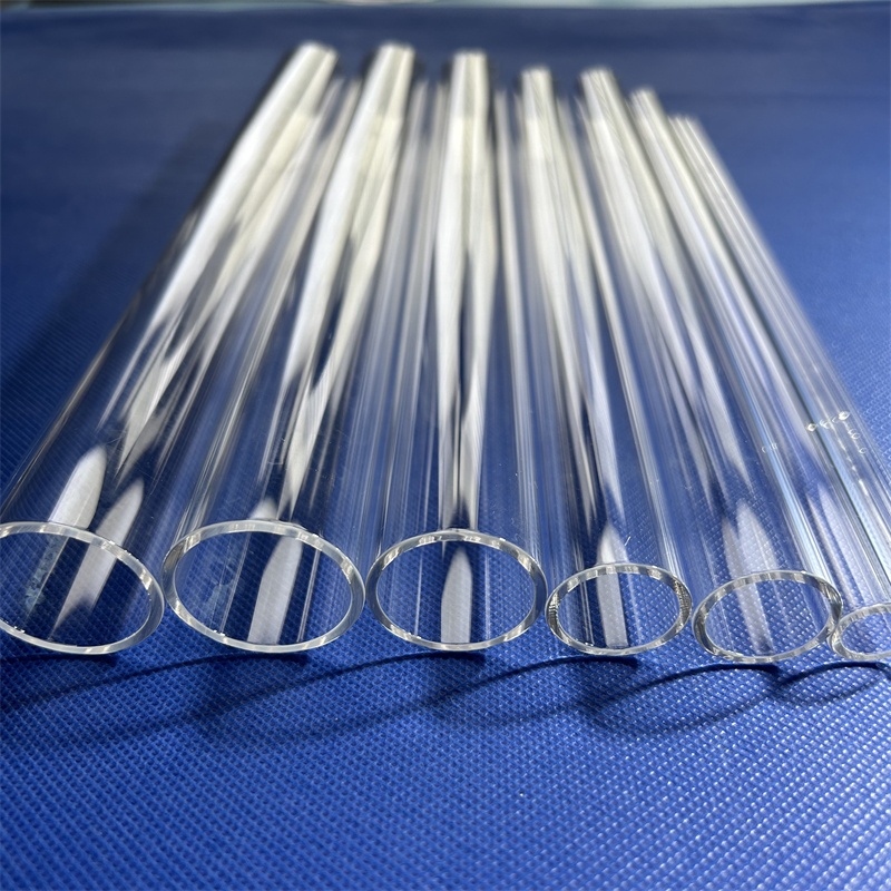 Furnace & Boiler
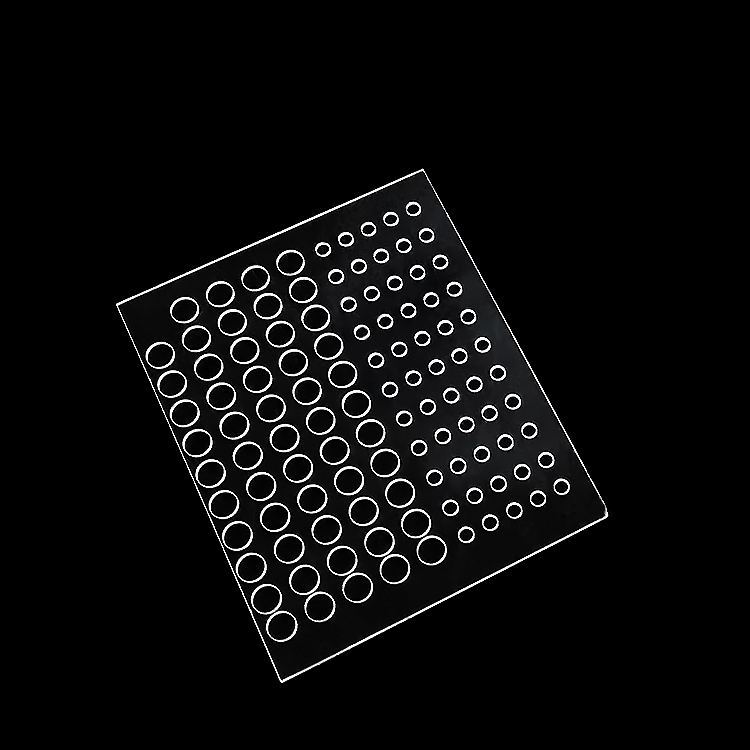 Optical JGS1/2/3
 Lab Instrument
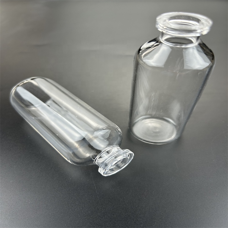 Medical & Chemical
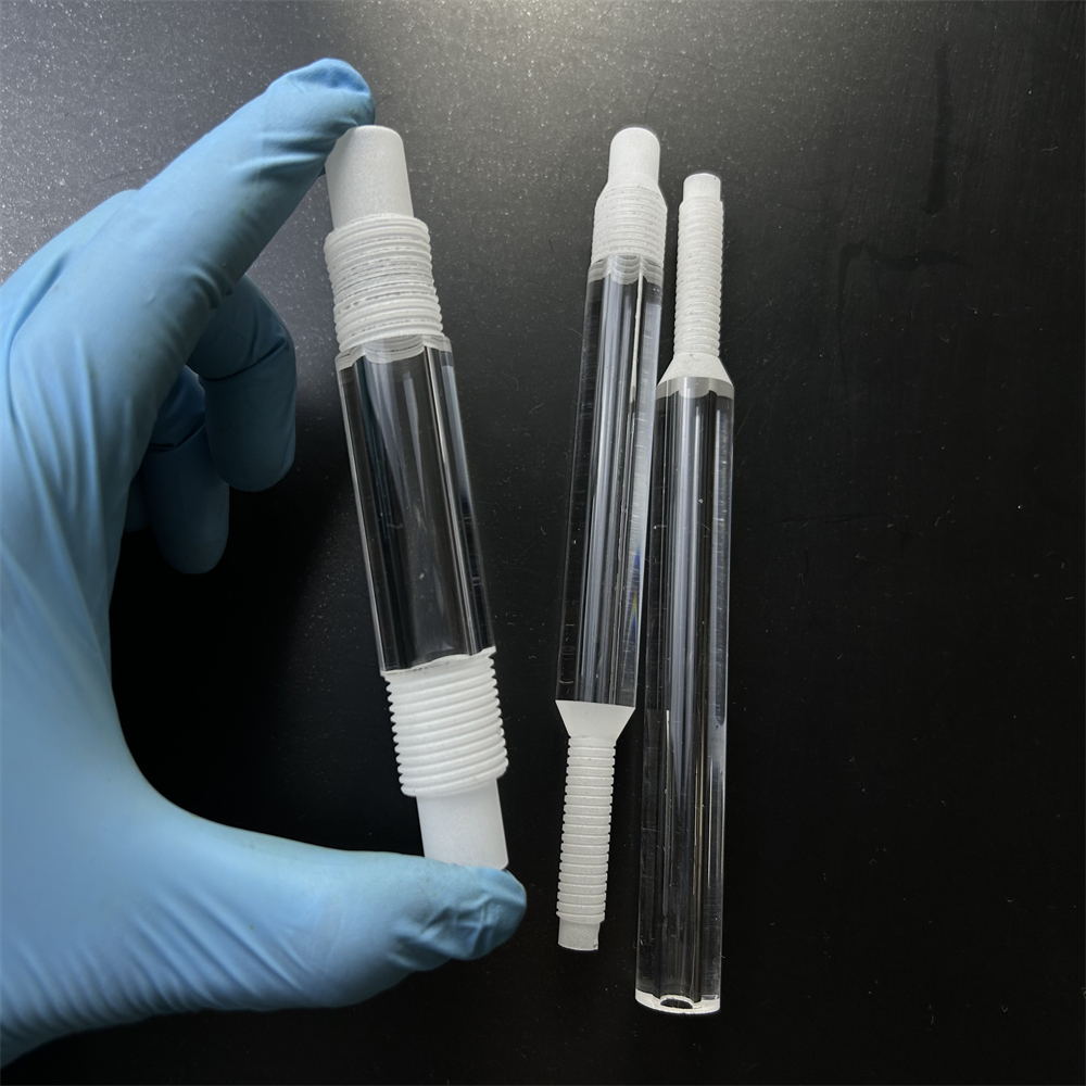 Precision Threading
Headquartered in Donghai County, Jiangsu Province—China's world-renowned "Crystal Capital"—Zunex Quartz Products Co., Ltd. merges geographical mineral access with high-end thermal and cold laser machining centers.
Positioned at the epicenter of China's quartz deposits, our refining processes eliminate transitional metallic impurities (Fe < 0.2 ppm, Al < 8 ppm, Ti < 1 ppm). This mineral purity guarantees high-temperature devitrification resistance and dielectric stability.
Beyond traditional manual diamond wire cutting, our workshop operates picosecond and femtosecond laser processing lines. We drill micro-holes (diameter ≥ 0.1 mm), shape intricate wafer carrier slots, and bevel edges with negligible thermal heat-affected zones (HAZ).
Whether your project requires complex double-walled quartz reaction vessels, BET sample twin tubes, flared flanges, or CNC-milled quartz plates, our engineering office turns CAD geometry into physical quartz parts in 3 to 7 working days.
Every hot-worked quartz element undergoes programmable electric furnace de-stressing at 1150°C followed by controlled ramp-down cooling. Polariscopic inspection verifies zero residual internal stress, preventing spontaneous shattering during high-pressure thermal cycling.
Supplying JGS1 synthetic silica, JGS2 fused quartz, and JGS3 infrared water-free quartz. Each shipment is paired with spectrographic transmission curves, surface roughness profilometry (Ra ≤ 0.2 nm capability), and dimensional verification reports.
Fused quartz glass is inherently brittle. We utilize multi-layer PE custom-molded foam inserts, vacuum-sealed barrier film, desiccant chambers, and ISPM-15 compliant reinforced plywood crates. Zero-breakage delivery is backed by insured ocean, air, and express logistics.
Selecting the appropriate fused silica or fused quartz substrate determines transmission efficiency, laser-induced damage thresholds (LIDT), and furnace operating lifetimes. Review our verified laboratory baseline parameters below.
In Chinese and international material specifications, fused silica glass is categorized based on its optical transmission spectrum, synthesis methodology, and hydroxyl ion (OH−) concentration.
| Property Parameter | JGS1 (Synthetic Fused Silica) | JGS2 (Optical Fused Quartz) | JGS3 (Infrared Fused Quartz) |
|---|---|---|---|
| Primary Raw Material | High-purity SiCl4 gas phase synthesis | Natural refined Donghai crystal quartz sand | Electric vacuum-fused low-OH quartz |
| Spectral Range | 185 nm – 2500 nm (Deep UV) | 220 nm – 2500 nm (UV-Vis) | 260 nm – 3500 nm (Infrared) |
| Hydroxyl (OH−) Content | High (≥ 800 – 1200 ppm) | Medium (30 – 150 ppm) | Ultra-Low (≤ 5 – 10 ppm) |
| 2730 nm IR Absorption Band | Strong structural absorption drop | Moderate absorption drop | Zero absorption valley (Clean IR pass) |
| Fluorescence (254nm excitation) | Extremely low / undetectable | Low to negligible | Negligible |
| Bubble & Inclusion Class | DIN 3140 Class 0 (Virtually bubble-free) | ISO 10110 Class 1–2 | ISO 10110 Class 1–2 |
| Typical Applications | Excimer lasers, semiconductor stepper windows, UV photolithography | Sight glasses, UV sterilization reactors, high-temp observation ports | FTIR spectroscopy windows, pyrometers, IR halogen twin heating emitters |
| Mechanical & Thermal Property | Standard Metric Value | Engineering Significance |
|---|---|---|
| Density (ρ) | 2.20 × 10³ kg/m3 | Lightweight structural optical rigidity |
| Coefficient of Thermal Expansion (CTE) | 5.5 × 10⁻⁷ / °C (20°C – 320°C) | Immunity to rapid thermal shock; 1/20th the expansion of borosilicate glass |
| Continuous Working Temperature | 1100 °C | Ideal for horizontal/vertical semiconductor diffusion furnaces |
| Short-Term Max Temperature | 1300 °C | Withstands peak spike anneal and RTP processes |
| Softening Point | 1683 °C | Structural integrity maintained far beyond standard industrial glasses |
| Annealing Point | 1215 °C | Critical threshold for thermal stress elimination |
| Compressive Strength | 1150 MPa | Exceptional load-bearing threshold under hydrostatic pressure |
| Dielectric Constant (ε at 1 MHz) | 3.75 | Ultra-low electrical loss tangent for high-frequency microwave windows |
Global supply chain leaders face escalating cleanroom standards, tighter raw material allocations, and evolving microelectronic thermal budgets. How international buyers are securing procurement resilience:
High-purity quartz sand is geographically concentrated. Sourcing directly from Donghai-based integrated manufacturers allows B2B procurement managers to bypass trading markups, insulate against feedstock crunches, and secure multi-year fixed-price lot reserves for semiconductor tubes and crucibles.
Traditional diamond CNC grinding creates microscopic edge fissures (micro-chipping > 50 μm) that cause catastrophic thermal failure under 1000°C LPCVD environments. Forward-thinking procurement teams are mandating cold picosecond laser cutting and hole-coring, keeping sub-surface cracks below 5 μm.
At sub-5nm semiconductor nodes, alkali and transition metal outgassing degrades wafer yields. Leading buyers require Inductively Coupled Plasma Mass Spectrometry (ICP-MS) certificates per batch, auditing Lithium (Li), Sodium (Na), Potassium (K), and Copper (Cu) below 0.1 ppm aggregate.
The expansion of N-type silicon wafer formats (M10/G12) requires quartz diffusion process tubes with inner diameters expanding beyond 400 mm and lengths up to 3000 mm. Buyers are consolidating contracts with factories operating heavy-duty multi-axis hot-glass lathes capable of zero-sag thermal shaping.
Academic institutes and fab R&D laboratories no longer tolerate 8-week tooling lead times. Sourcing contracts are awarded to suppliers running digital automated CAM workflows that machine quartz flange fittings, BET tubes, and multi-well quartz plates directly from STEP drawings within 72 hours.
With sustainability and ESG mandates governing international trade, global fabs are prioritizing closed-loop quartz component recycling. Factories offering chemical cleanroom de-flaking, re-annealing, and precision flame refacing reduce capital expenditure by up to 35% compared to complete tooling replacement.
How manufacturing advancements are transforming raw silicon dioxide into ultra-high reliability solutions for aerospace, plasma etch chambers, and analytical chemistry.
Halogen-based plasma etching (CF4, NF3, Cl2) aggressively erodes bare fused quartz viewports and chamber liners. State-of-the-art quartz components now feature yttrium oxide (Y2O3) and alumina protective coatings, extending service life in corrosive plasma chambers by 400%.
By introducing trace titanium dopants during flame synthesis, quartz tubes effectively absorb harmful short-wave UV radiation (184.9 nm) while maximizing bactericidal 253.7 nm output. This enables high-intensity ozone-free UV disinfection lamps for public HVAC and water purification systems.
Overcoming quartz's ultra-low thermal expansion to match stainless steel or kovar flanges has historically required intermediate graded seals. Modern laser annealing and precision CNC grinding now enable direct-threaded quartz connections and glass-to-metal vacuum seals leak-tight to < 1 × 10⁻⁹ mbar·L/s.
Critical design parameters, material grades, tolerance verifications, and logistics protocols answered by our chief quartz glass engineers.
Yes. Our CNC machining centers and cold laser finishing systems interface directly with STEP, IGES, DWG, DXF, and PDF formats. Our engineering team reviews wall thicknesses, draft angles, and thermal stress points, issuing a comprehensive manufacturability confirmation and quotation within two hours.
Standard high-purity clear fused quartz operates continuously at 1100°C and withstands short-duration peaks up to 1300°C. Devitrification (crystallization into cristobalite) typically occurs above 1150°C if the surface is contaminated by alkali salts or fingerprints. Thorough cleaning and de-ionized water rinsing prevent premature surface nucleation.
JGS1 is synthetic silica synthesized via SiCl4, providing >90% transmission down to 185 nm, making it the choice for DUV optics and excimer lasers. JGS2 is derived from natural refined quartz and performs optimally in the 220 nm – 2500 nm range. JGS3 is vacuum-melted to strip hydroxyl groups (≤5 ppm OH), eliminating the 2.73 μm absorption band for infrared transmission up to 3.5 μm.
For optical windows and plates, we achieve thickness tolerances down to ±0.01 mm, surface flatness of λ/4 to λ/10 per 25 mm, and surface roughness (Ra) below 0.2 nm. For extruded and blown tubes, standard outside diameter (OD) tolerance is ±0.5% with precision re-drawn options held to ±0.05 mm.
While borosilicate softens around 820°C and has a CTE of 33 × 10−7 / °C, fused quartz softens at 1683°C and has a CTE of 5.5 × 10⁻⁷ / °C. Fused quartz can be heated red-hot to 1100°C and plunged directly into ice water without cracking. Additionally, quartz has superior chemical resistance to all mineral acids except hydrofluoric and concentrated hot phosphoric acid.
We implement custom shock-absorbing foam molds calibrated to the component's geometry. Tubes are internally supported and nested in rigid PVC protective sleeves. The entire assembly is sealed in moisture-barrier bags with desiccant and secured within heavy-duty export plywood crates featuring outer shock indicators.
We maintain a flexible manufacturing schedule with an MOQ of 1 piece for prototype research drawings, pilot testing, and proof-of-concept projects. High-volume continuous production runs for OEM furnace builders, UV lamp manufacturers, and semiconductor equipment integrators are supported with batch discounting.
Yes. Every production run is inspected by our quality assurance lab using coordinate measuring machines (CMM), spectrophotometers, and polariscopic stress gauges. On request, we provide certified ICP-MS chemical composition reports verifying metallic trace elements, RoHS/REACH compliance documentation, and full dimensional inspection sheets.
Send your CAD drawings, required material grade (JGS1, JGS2, JGS3, or Clear Fused Quartz), dimensional tolerances, and planned batch volumes. Our factory engineers in Donghai will review your design and return an itemized quotation within 2 hours.