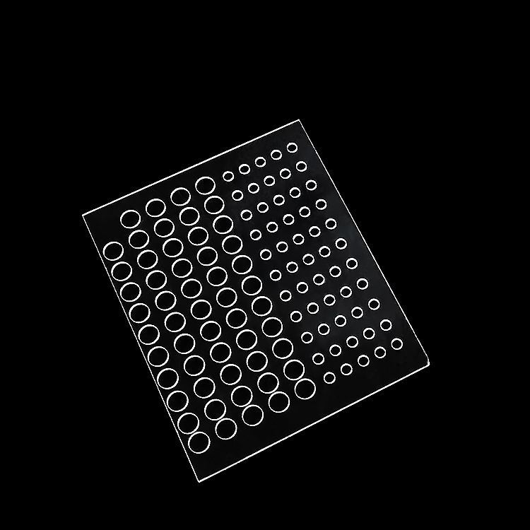
High-Temperature Optics Grade Fused Quartz Glass Plate
JGS1 / JGS2 / JGS3
0.5 - 100mm Thickness
λ/4 Surface Flatness
Engineered in Donghai County—China's crystal industrial center—to meet stringent semiconductor fab thermal specifications, excimer laser thresholds, and chemical vacuum containment.
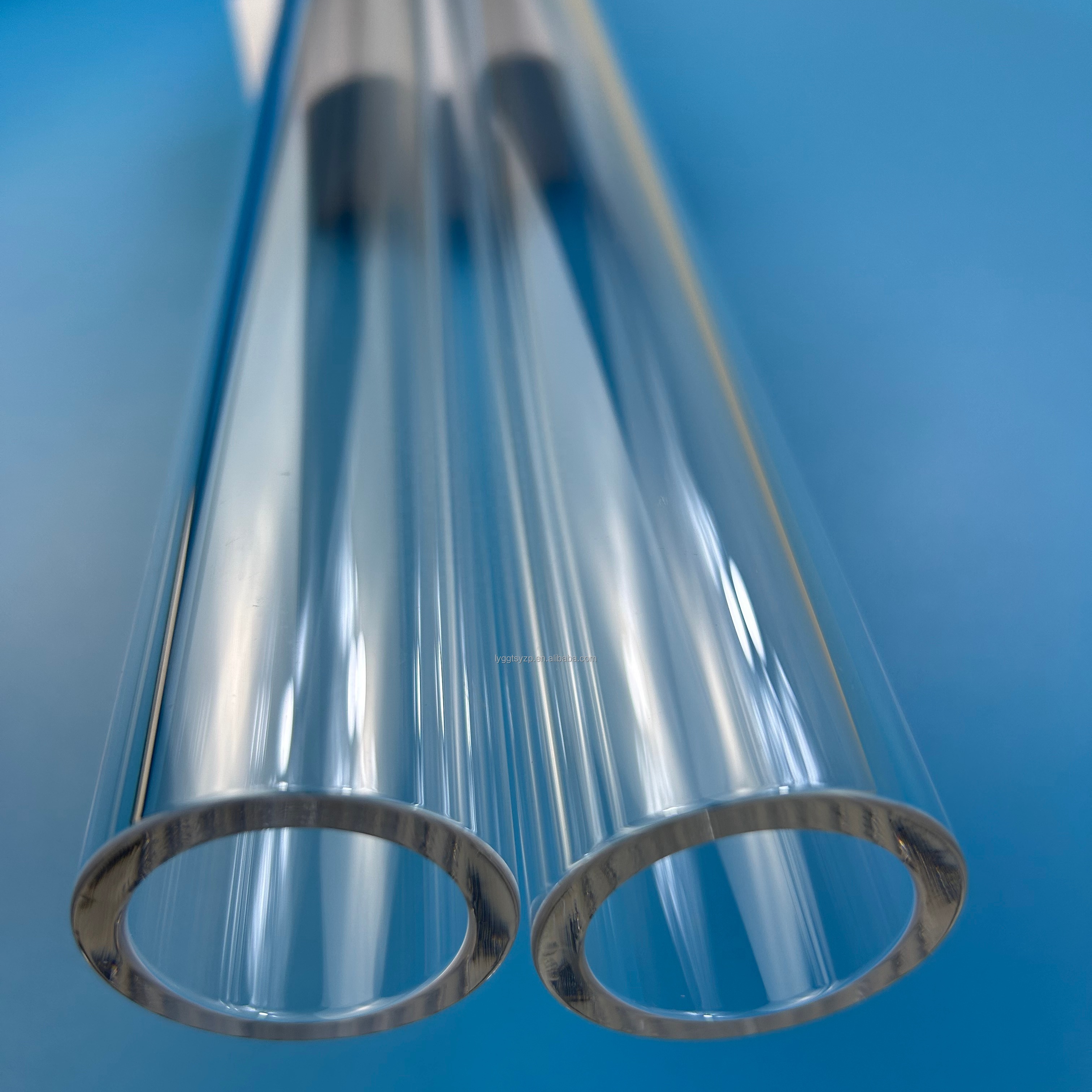
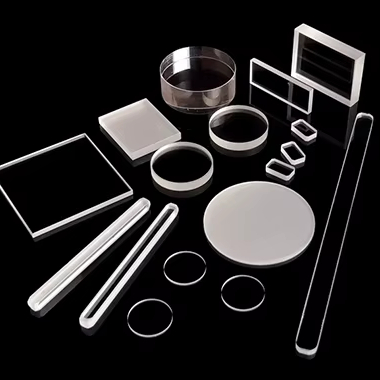

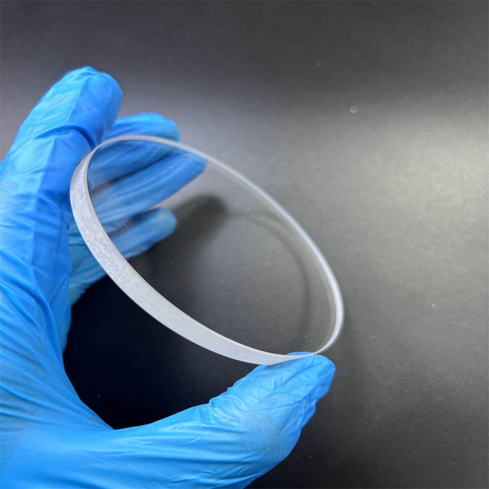
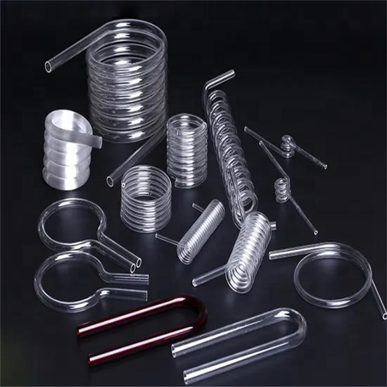
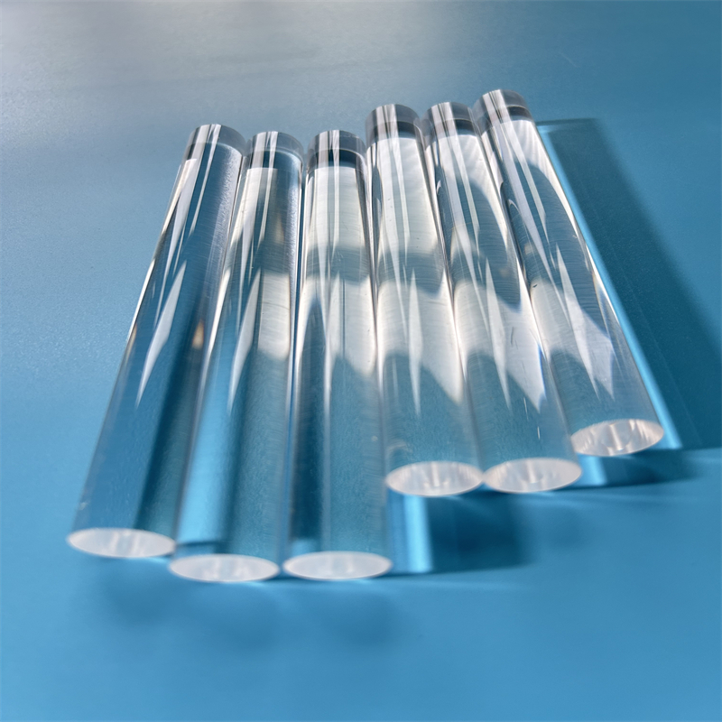
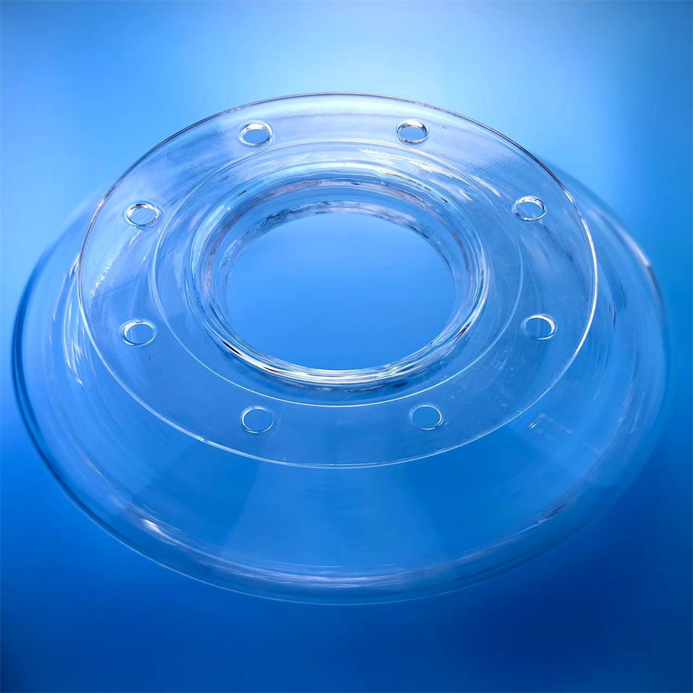
Combining proprietary high-temperature hydrogen-oxygen flame refining, 5-axis CNC ultrasonic diamond grinding, and cleanroom vacuum packaging.
Directly headquartered in Donghai County, we leverage premier high-purity natural silica sand (≥99.99% SiO2) and vapor-synthesized silicon tetrachloride precursors to eliminate metallic contaminants.
Equipped with state-of-the-art CO2 and femtosecond laser processing setups to execute micro-hole drilling (Ø<0.2mm), edge beveling, micro-fluidic grooving, and crack-free wafer cutting.
100% of incoming customer engineering schematics (DWG, STEP, DXF, PDF) undergo rapid DFM (Design for Manufacturability) verification within 2 hours, preventing structural thermal fatigue downline.
Every fragile fused quartz assembly is shielded with vacuum poly-wrap, bespoke CNC cut-to-fit EVA shock-absorbing foam, and heavy-duty multi-layer fumigated wooden export crating.
A comprehensive technical comparison to assist optical engineers, vacuum furnace builders, and chemical apparatus designers in specifying the exact glass matrix.
| Physical / Thermal Parameter | Standard Value | Test / Inspection Standard |
|---|---|---|
| Chemical Purity (SiO2) | ≥ 99.99% (Electronic Grade ≥ 99.999%) | ICP-OES / GD-MS Spectrometry |
| Density (ρ) | 2.20 ± 0.02 g/cm³ | Archimedes Immersion Method |
| Softening Point | 1683 °C ± 15 °C | ASTM C338 Standard |
| Annealing Point | 1215 °C ± 10 °C | ASTM C336 Standard |
| Strain Point | 1120 °C ± 10 °C | Beam-Bending Viscosimeter |
| Linear Expansion Coeff. (CTE) | 5.5 × 10⁻⁷ / °C (20°C - 320°C) | Dilatometric Interferometry |
| Thermal Shock Resistance | Drop from 1100°C into 20°C water without crack | Rapid Quench Test |
| Dielectric Strength (20°C, 1MHz) | 25 - 40 kV/mm | IEC 60243-1 High Voltage Test |
| Refractive Index (nd @ 589.3 nm) | 1.45846 | Abbe Refractometry |
Produced by chemical vapor deposition of SiCl4. Virtually free of bubbles and metallic impurities. Ideal for excimer stepper optics, UV photolithography windows, laser mirrors, and fluorescence spectroscopy cuvettes.
Smelted from purified natural crystalline silica under oxy-hydrogen flame. Delivers high visual transmission across UV-Vis spectrum. Preferred for sight glasses, UV curing lamps, and semiconductor diffusion tubes.
Vacuum-melted quartz glass with strictly suppressed hydroxyl content (OH ≤ 2 - 5 ppm). Eliminates the destructive 2.73μm OH absorption band. Designed for short-wave/medium-wave IR heaters and thermal imagers.
Key technical shifts shaping fused silica sourcing in the semiconductor wafer fabrication, quantum communications, and renewable energy sectors through 2026-2030.
As semiconductor lithography nodes advance past 3nm and gate-all-around (GAA) architectures scale, demand for ultra-flat fused silica wafer carriers and EUV pellicle substrates has accelerated.
Photovoltaic N-type TOPCon/HJT cell expansions and third-generation SiC/GaN power electronics necessitate oversized quartz furnace tubes and flanged reactors with extreme dimensional stability.
Global R&D centers and high-mix low-volume (HMLV) semiconductor test facilities are replacing massive inventory stockpiles with direct-to-factory precision digital machining.
Direct technical answers addressing material integrity, machining tolerances, thermal stress, and quotation workflows.
While often used interchangeably, "Fused Quartz" is typically produced by melting natural, high-purity crystalline quartz rock (SiO2 content approx. 99.99%). In contrast, "Synthetic Fused Silica" (such as JGS1) is synthesized chemically using silicon tetrachloride (SiCl4) gas in a flame hydrolysis process. Synthetic fused silica boasts superior deep ultraviolet transmittance down to 185 nm and virtually zero heavy metal impurities (Fe, Al, Ti < 0.1 ppm).
Devitrification occurs when surface alkaline impurities (sodium, potassium, calcium) act as nucleation sites to convert amorphous silica into cristobalite. We prevent this by conducting ultra-pure deionized water ultrasonic washings, acid etching (hydrofluoric-nitric blend) to strip all surface micro-contaminants, and high-purity annealing cycles before vacuum packaging.
For custom quartz windows, discs, and diffusion tubes, our standard CNC milling and laser finishing holds outer diameter/length tolerances within ±0.05 mm. For high-precision semiconductor wafers and optical viewports, we routinely achieve dimensional tolerances of ±0.01 mm, parallelism < 10 arcseconds, and surface roughness Ra < 0.5 nm.
Yes. Our master glassblowers execute intricate hydrogen-oxygen lathe welding of NW/KF flanges, CF conflat flanges, twin-tube emitter assemblies, and spiral capillary coils. All weld junctions undergo fine-annealing in computer-controlled electric kilns to thoroughly relieve localized thermal hoop stresses.
With our verified 100% response rate on Alibaba and global trade portals, all engineering drawing submissions (PDF, CAD, DXF, or STEP) are reviewed by our senior technical team with formal DFM feedback and competitive factory-direct quotes issued within 2 hours.
Every single glass unit is cleanroom cleaned, wrapped in static-free surface film, nested inside custom CNC-routed high-density EVA foam cushions, and enclosed in double-wall reinforced cartons or customized plywood crates certified to ISTA-3A drop test criteria.
Contact our Donghai production engineering facility directly. Receive instant material guidance, tolerance evaluations, and tiered batch pricing within 2 hours.