Precision Quartz Fabrication Portfolio
Direct from our Donghai facility: Custom engineered fused silica and quartz ware tailored to stringent semiconductor, optics, and extreme thermal processing tolerances.
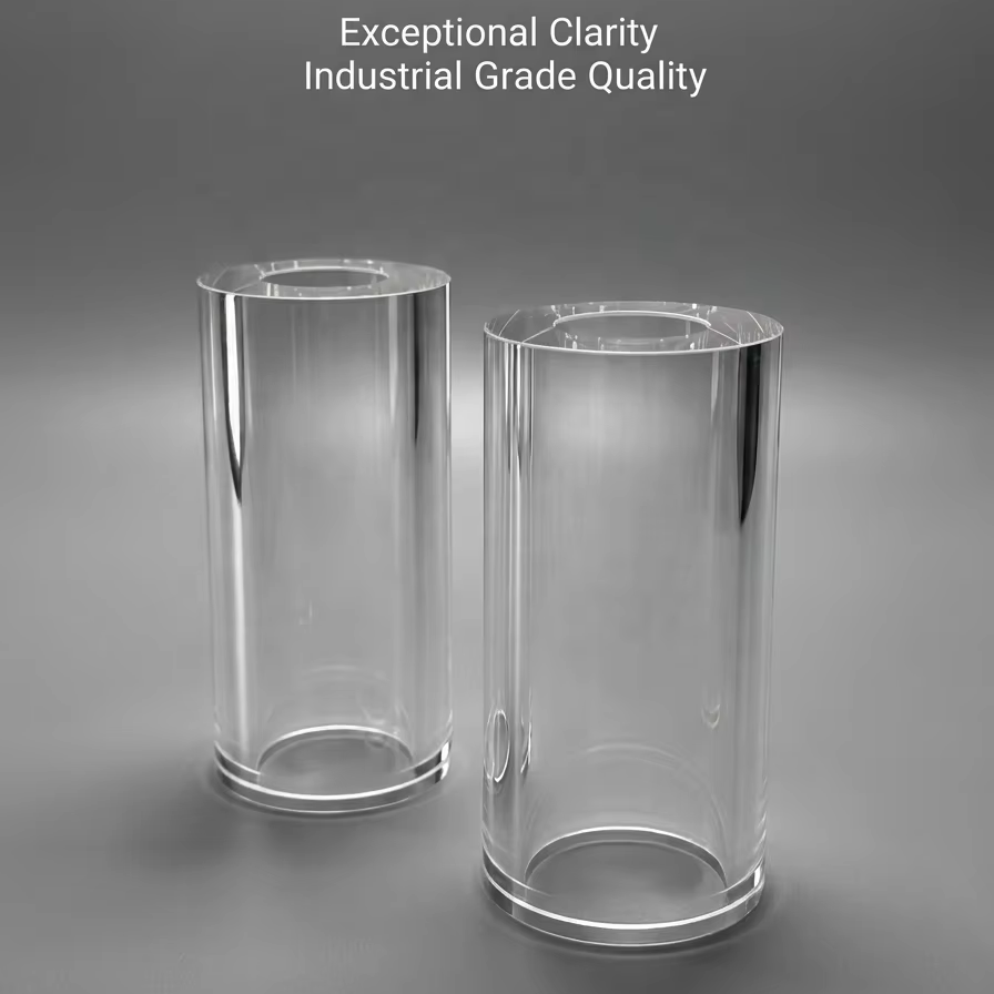
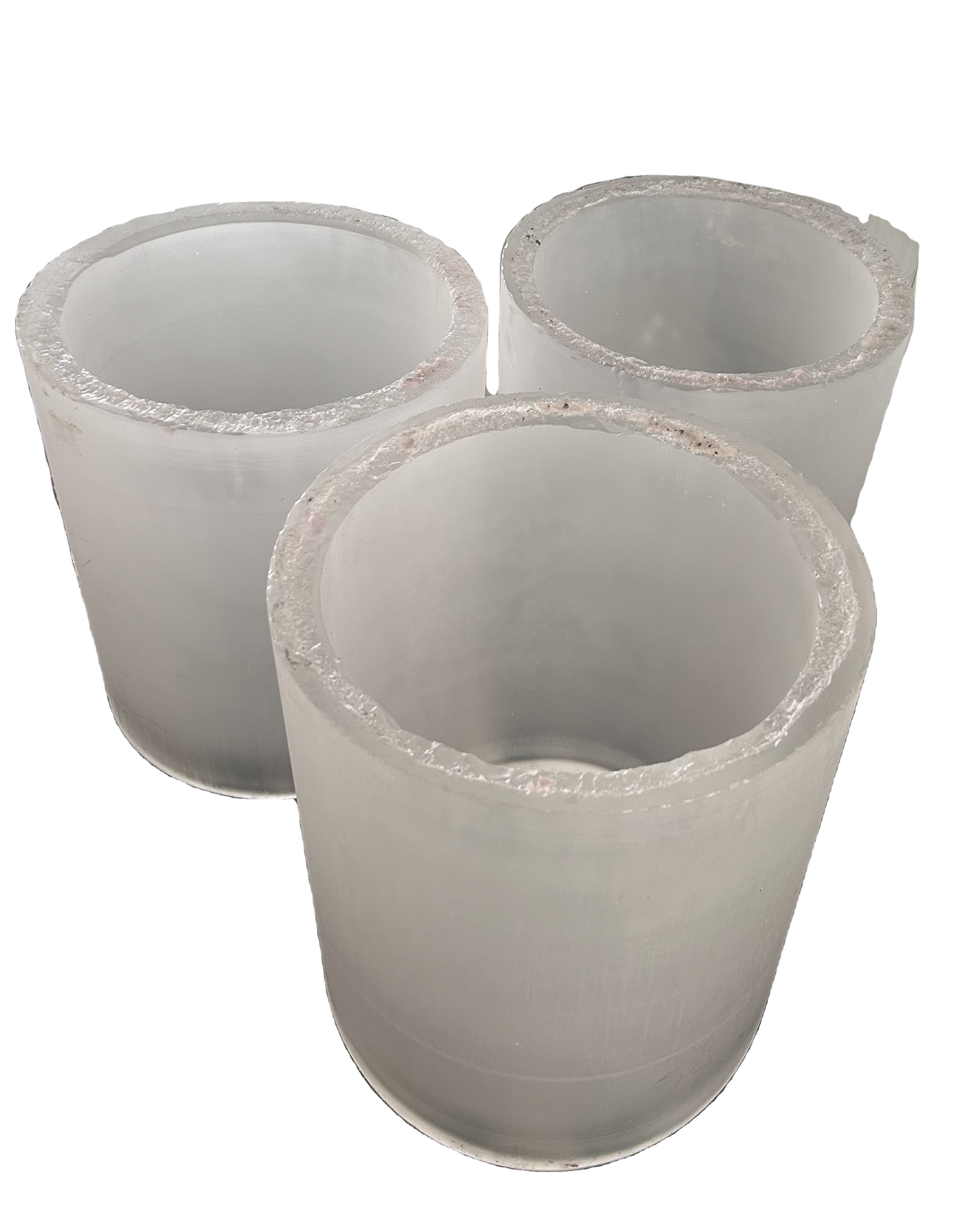
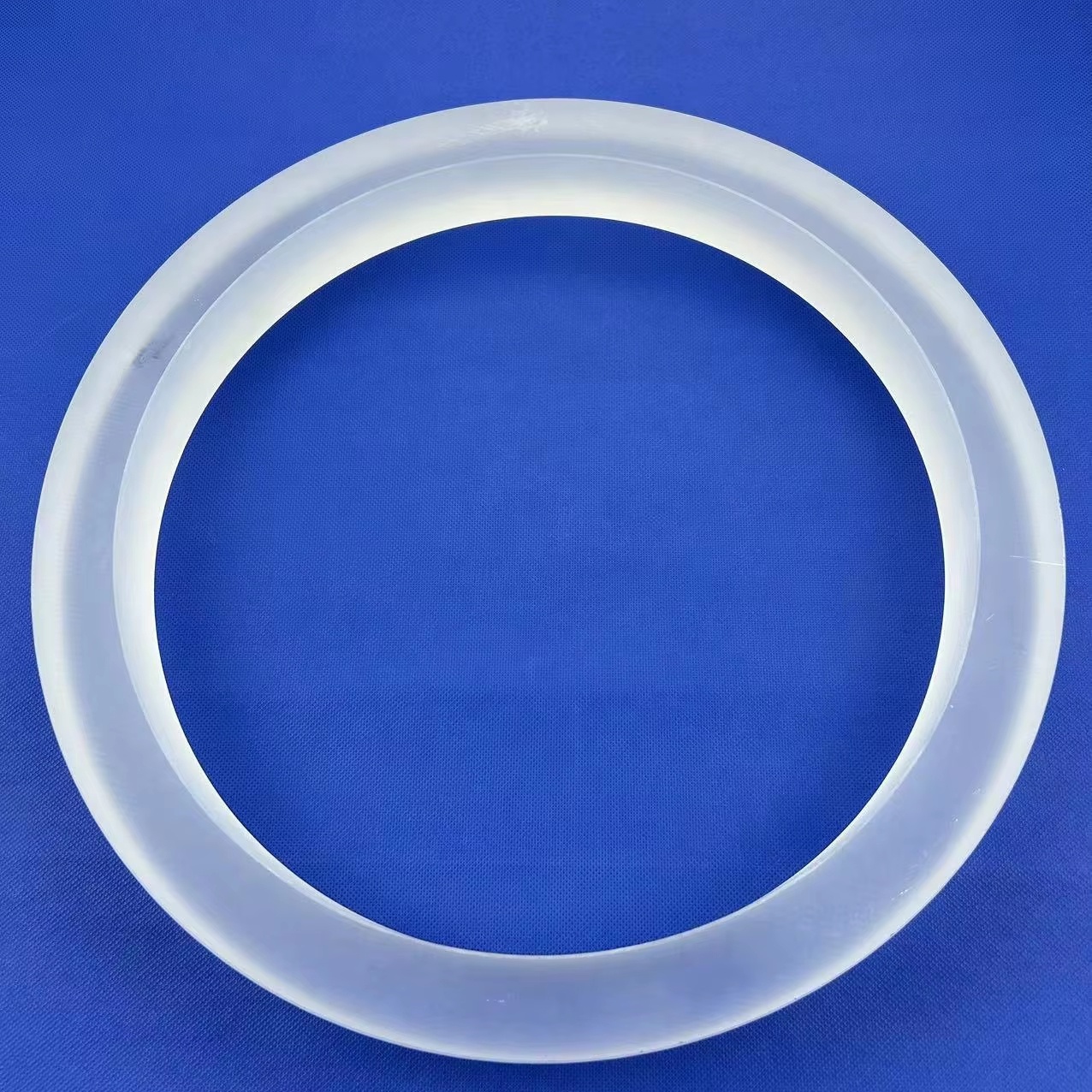
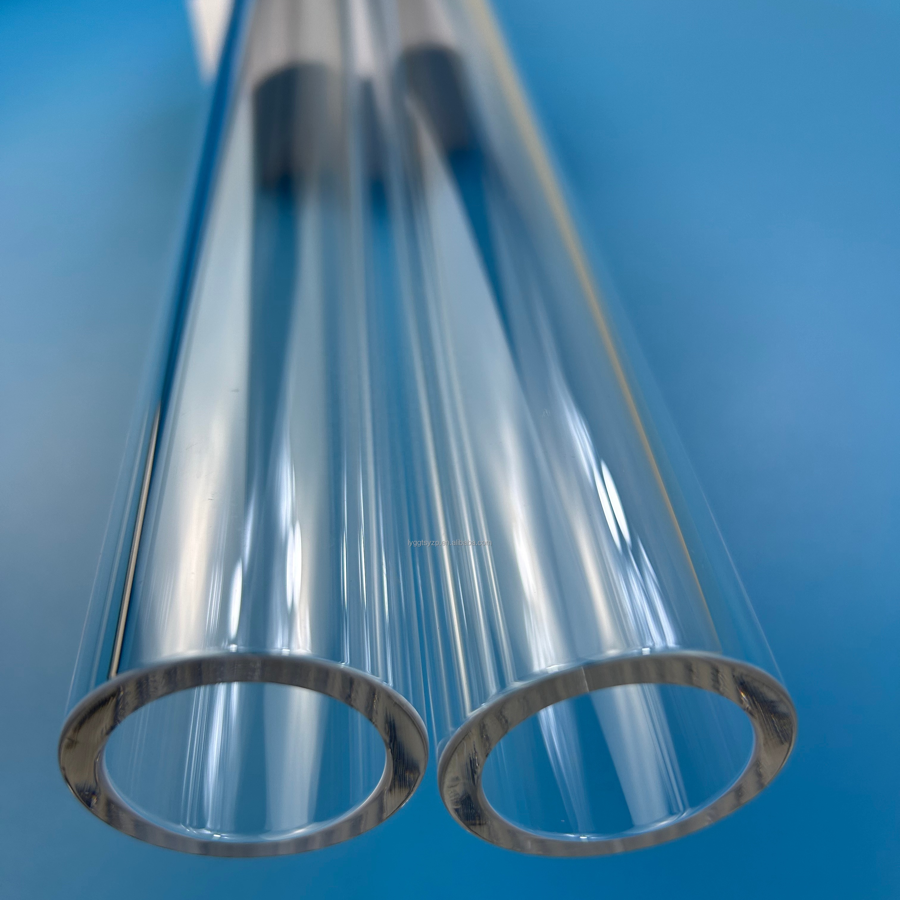
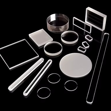
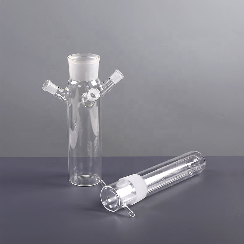
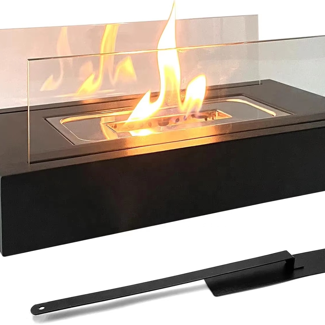
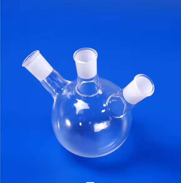
Engineered in China's Crystal Capital: Why Choose Zunex
Direct manufacturing execution combining high-grade mineral assets from Donghai County with aerospace-level machining tolerances.
Regional Geolocation Edge
Located in Donghai County, China's world-famous crystal and silicon resource hub, providing uncompromised access to premium mineral grade raw quartz ingots.
Laser Micro-Finishing
Proprietary quartz laser drilling, sub-millimeter grooving, slotting, and precision edge-chamfering preventing micro-fractures under extreme thermal cycles.
Rigorous Customization
Direct fabrication to CAD, DWG, and STEP specifications. Every custom geometry is vetted by our optical application engineers within 2 hours of RFQ arrival.
Verified Export Credibility
Alibaba-audited manufacturer operating under rigorous ISO-standard QC with cleanroom visual inspection, high-shock packaging, and global logistics dispatch.
Technical White Paper: Fused Silica Substrates & Wafer Manufacturing
Authoritative analysis of material composition, chemical resilience, optical spectral bands, and thermal endurance for advanced engineering buyers.
In modern microelectronics, optoelectronics, and micro-electro-mechanical systems (MEMS), the specification of synthetic fused silica and natural fused quartz wafers is critical. As device geometries shrink past sub-micron regimes and operating temperatures in dry-etching and chemical vapor deposition (CVD) escalate, standard borosilicate or aluminosilicate glasses fail catastrophically due to thermal expansion mismatch and alkali ion diffusion. This white paper serves as a comprehensive procurement framework for enterprise sourcing teams evaluating wholesale Chinese quartz wafer production capabilities.
Material Grade Classification: JGS1 vs. JGS2 vs. JGS3
The transmission spectra and intrinsic purity of fused quartz are fundamentally determined by the feed-gas precursor or crystalline quartz source employed during synthesis. Industrial purchasers must select the proper JGS classification based on wavelength transparency and hydroxyl (OH-) content:
- JGS1 (Synthetic Fused Silica): Synthesized via chemical flame hydrolysis of high-purity silicon halides (SiCl4). Characterized by absolute chemical purity (>99.999% SiO2) and virtually zero metallic impurities (Fe, Al, Ti < 0.1 ppm). It boasts superior transmission in the deep ultraviolet (DUV) range (185 nm – 2500 nm) and is inherently bubble- and inclusion-free, making it the premier choice for DUV photolithography masks, excimer laser windows, and optical wafers.
- JGS2 (Optical Grade Fused Quartz): Melted from natural refined quartz crystals utilizing electric fusion or oxyhydrogen flames. Provides broad optical transparency across the UV-Visible range (220 nm – 2500 nm). Widely deployed for semiconductor diffusion furnace viewing ports, wafer carriers, analytical cuvettes, and standard lithography dummy substrates.
- JGS3 (Infrared Grade Fused Quartz): Synthesized through vacuum electro-fusion methods that dramatically eliminate structural hydroxyl (OH-) ions (typically below 5 ppm). This suppression of the 2.73 μm absorption band grants JGS3 unmatched transmission extending deep into the infrared spectrum (260 nm – 3500 nm), optimal for thermal imaging systems, pyrometry viewports, and intense infrared heater assemblies.
| Physical / Chemical Property | Standard Fused Quartz (JGS2) | Synthetic Fused Silica (JGS1) | IR Fused Silica (JGS3) |
|---|---|---|---|
| Chemical Purity (SiO2) | ≥ 99.99% | ≥ 99.9999% | ≥ 99.995% |
| Hydroxyl (OH-) Content | 150 – 200 ppm | 800 – 1200 ppm | ≤ 5 ppm |
| Spectral Window (>80% T) | 220 nm – 2500 nm | 185 nm – 2500 nm | 260 nm – 3500 nm |
| Coefficient of Thermal Expansion (0-300°C) | 5.5 × 10^-7 /°C | 5.2 × 10^-7 /°C | 5.5 × 10^-7 /°C |
| Continuous Working Temp / Softening Point | 1100°C / 1683°C | 1150°C / 1730°C | 1100°C / 1680°C |
| Surface Roughness (Polished Wafer Ra) | < 0.5 nm (Super-polished) | < 0.2 nm (Atomic Grade) | < 0.8 nm |
Precision Machining: Thermal Integrity vs. Micro-Cracking
Fabricating mechanical geometries from fused quartz — such as wafer carrier slots, twin-tube configurations, custom flange ports, and edge bevels — requires rigorous stress management. Traditional mechanical dicing and mechanical drilling exert heavy shear stress, introducing micro-cracking along the perimeter. When subjected to rapid thermal annealing (RTA) or corrosive chemical vapor deposition atmospheres (containing gases such as HF, Cl2, or NF3), these micro-cracks propagate, leading to catastrophic wafer fracturing.
At Zunex, we deploy dual-axis CO2 and picosecond laser drilling and profiling combined with full-flame annealing. Our post-machining chemical etching dissolves micro-fissures, relieving residual thermal stress and restoring mechanical rupture resistance to 100% of theoretical threshold limits.
Future Procurement & Technological Trends
Emerging industry movements driving strategic sourcing shifts in global semiconductor and photonic fabrication.
1. Demand for Ultra-Thin & Large-Diameter Wafers
The proliferation of 3D IC packaging, advanced silicon photonics (SiPh), and wafer-level optics is driving transition from standard 4-inch and 6-inch quartz substrates toward ultra-flat 8-inch and 12-inch wafers with total thickness variation (TTV) under 1.5 micrometers.
2. Direct Supply Chain Vertical Integration
International OEMs are moving away from multi-tiered brokerage houses. Procurement directors are partnering directly with high-volume Chinese manufacturing facilities that control hot-fusion, cold-grinding, CNC milling, and class 1000 cleanroom packaging under one roof.
3. Harsh Environment Plasma & Fluorine Resistance
Next-generation dry-etch processes utilizing aggressive halogen plasmas require hyper-pure, bubble-free fused silica components. The elimination of particulate micro-inclusions minimizes localized etching pits and extends component lifecycle in high-density plasma reactors.
Frequently Asked Questions for B2B Procurement
Clear, definitive answers to technical and logistics considerations encountered during procurement audits.
Can Zunex manufacture custom quartz wafers strictly from technical CAD drawings?
Yes. Custom OEM fabrication is our fundamental strength. We process CAD files (.DWG, .DXF, .STEP, .PDF), matching exacting dimensional tolerances up to ±0.005mm, customized flat/notch orientations (SEMI standard), edge chamfers, and specialty surface finishes.
What surface roughness (Ra) and flatness (TTV) parameters can you achieve?
Our double-sided mechanical and chemical-mechanical polishing (CMP) processes achieve optical surface qualities of 20/10 Scratch/Dig, surface roughness Ra < 0.5 nm, total thickness variation (TTV) < 2 μm, and bow/warp < 10 μm across standard 100mm to 300mm wafer formats.
How do you prevent brittle fracturing during international freight handling?
All finished optical quartz wafers and precision tubes are vacuum-sealed in cleanroom cassettes or customized ESD antistatic trays, suspended inside multi-layered shock-absorbing EPE closed-cell foam, and crated in export-grade reinforced wooden cases compliant with ISPM 15 standards.
What quality control documentation accompanies wholesale shipments?
Every commercial batch is accompanied by comprehensive quality assurance documentation, including full Spectrophotometer Transmission Curves, Certificate of Analysis (CoA) for raw SiO2 purity, 3D coordinate measuring machine (CMM) dimensional reports, and cleanroom packaging certifications.
Accelerate Your Quartz Wafer Procurement Project
Submit your CAD blueprints, thickness requirements, and annual volume estimates. Our senior quartz engineering team will review manufacturability, optimize processing routes, and return a competitive direct-factory quotation within 2 hours.
Contact Us