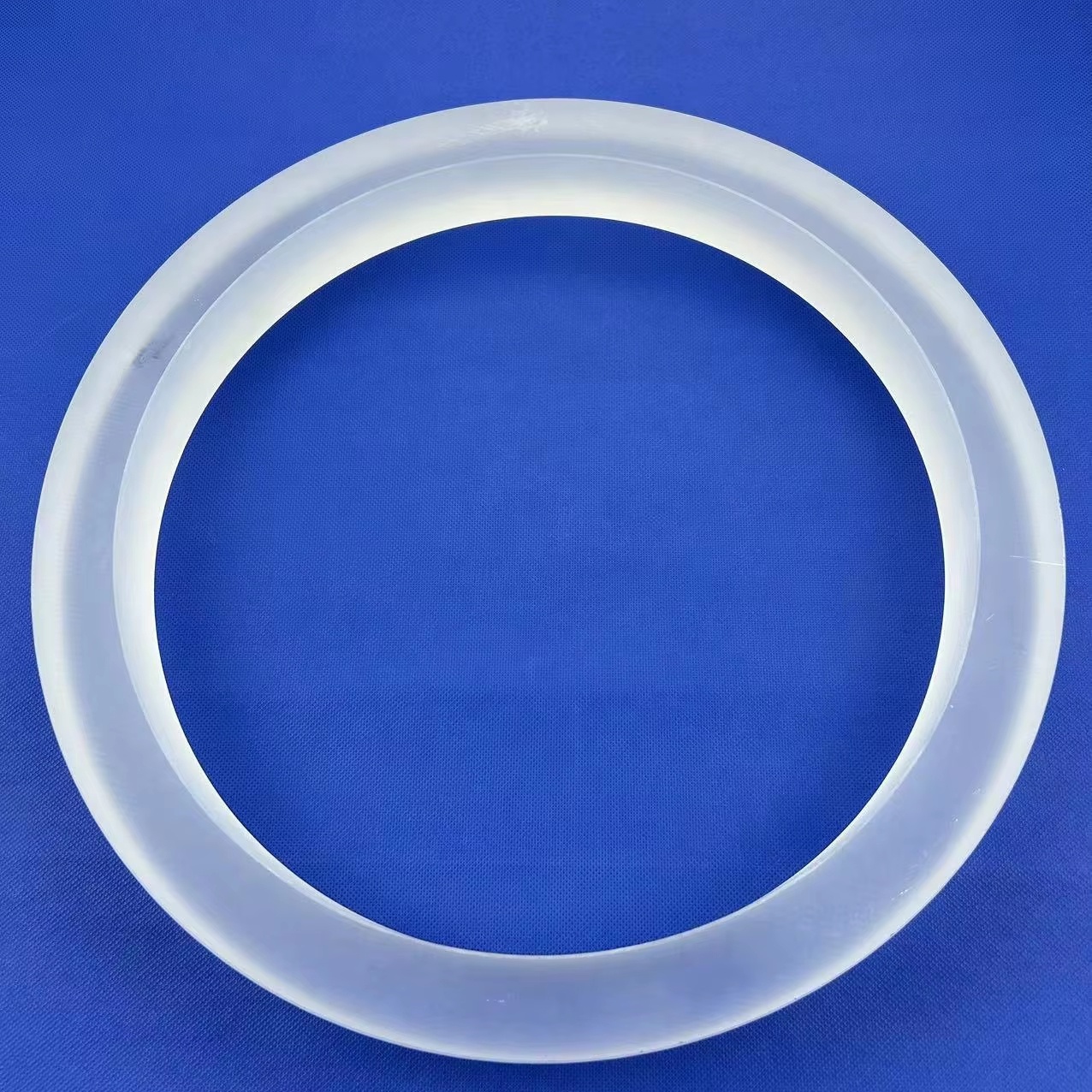
High-Precision Quartz Ware
Precision Substrates & Fabricated Quartz Solutions
Engineered from 99.99% high-purity SiO₂ feedstocks to deliver flawless mechanical endurance, thermal shock resistance, and unmatched spectral throughput across semiconductor, solar PV, and UV-IR optics.
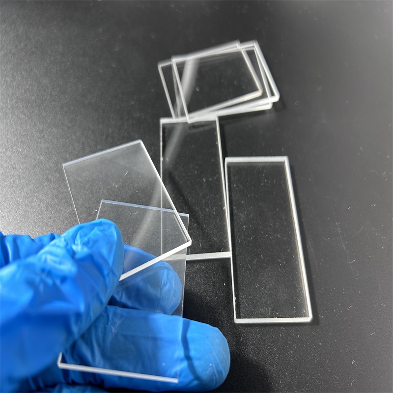
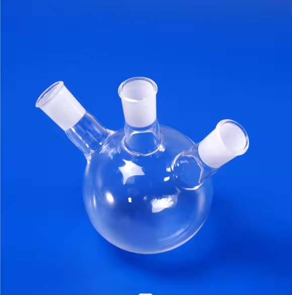
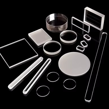
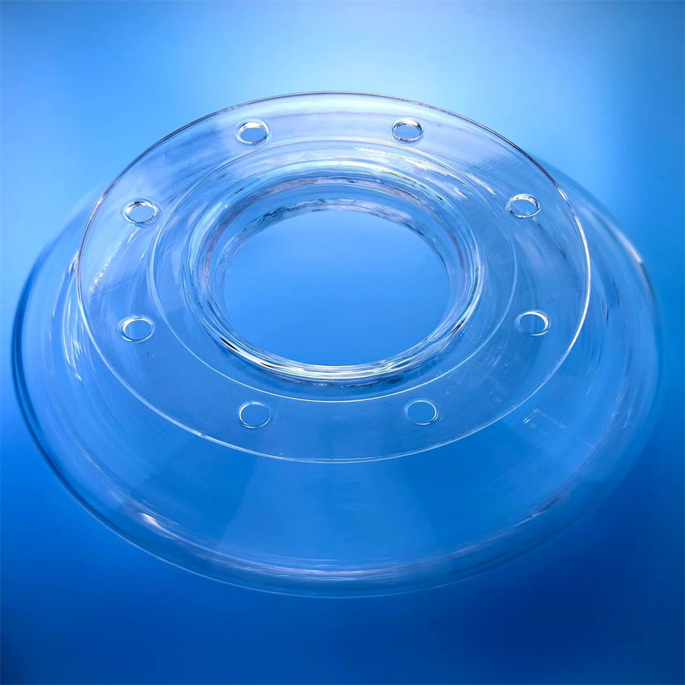
Engineering Whitepaper
Material Science & Substrate Fabrication Metrology
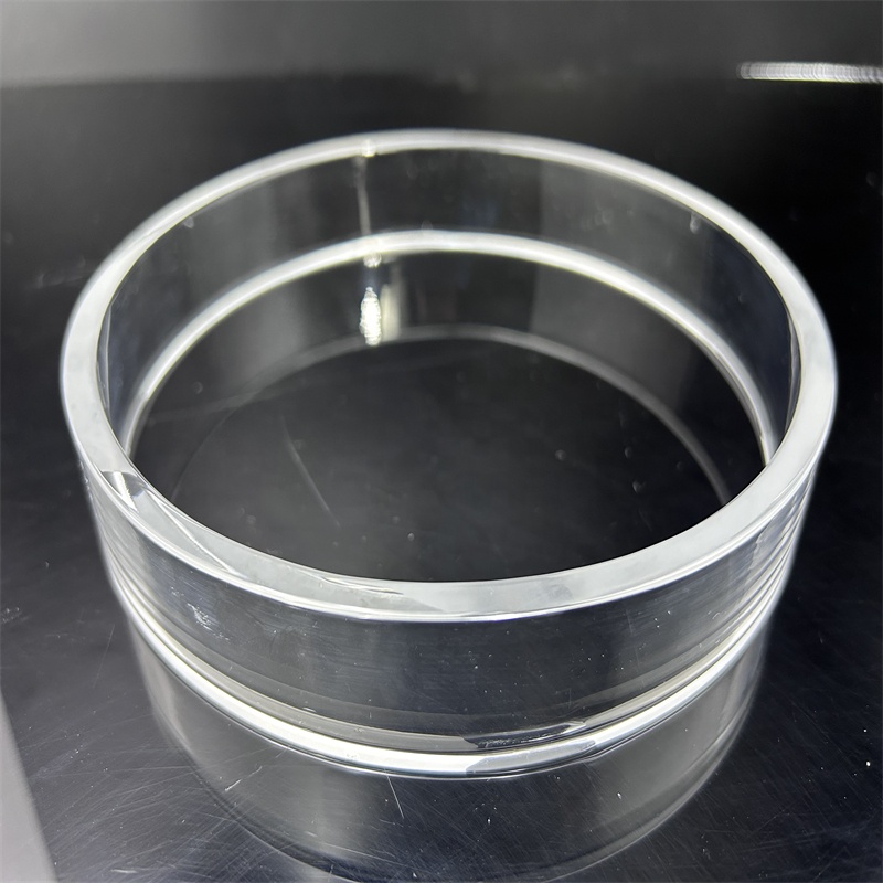
A comprehensive technical evaluation comparing synthetic fused silica against natural quartz crystal matrices for ultra-precision semiconductor wafer handling, laser optics, and microfluidics.
Material Classification & Grade Selection
The choice between natural fused quartz and chemical-vapor-deposited synthetic fused silica determines refractive index homogeneity, hydroxyl (OH⁻) group absorption bands, and laser damage thresholds (LIDT):
- JGS1 (Synthetic Fused Silica): Manufactured via SiCl₄ flame hydrolysis. Virtually free from metallic bubbles and inclusions. Yields continuous, high deep-UV transmission down to 185 nm, making it indispensable for 193 nm/248 nm photolithography masks, excimer laser optics, and microfluidic bio-chips.
- JGS2 (Optical Grade Fused Quartz): Smelted from premium natural rock crystals. Shows superior optical transmission across 220 nm – 2500 nm, standardly chosen for sight windows, solar crucible viewports, and UV lamp jackets.
- JGS3 (Infrared Grade Fused Silica): Vacuum-melted with extremely depleted OH content (< 5 ppm). Eliminates the classic 2.73 μm hydroxyl absorption valley, delivering uniform transmission through the mid-wave infrared spectrum up to 3500 nm.
Metrological Benchmarks & Physical Parameters
| Physical / Thermal Metric | Standard Value | Testing Protocol |
|---|---|---|
| Chemical Purity (SiO₂) | ≥ 99.99% (Low Metallic Ions) | ICP-MS Chemical Assay |
| Coefficient of Thermal Expansion | 5.5 × 10⁻⁷ / °C (20–320°C) | Dilatometric Metrology |
| Thermal Shock Resistance | ΔT > 1100 °C (Water Quench) | High-Temp Furnace Stress |
| Refractive Index (nd @ 589.3nm) | 1.45846 ± 0.0001 | V-Prism Refractometer |
| Surface Roughness (Ra) | ≤ 0.5 nm (Super-Polished) | Atomic Force Microscope (AFM) |
| Surface Quality / Transmissivity | 10-5 Scratch-Dig / >92% (Uncoated) | MIL-PRF-13830B Spectrophotometry |
Direct Manufacturer Strengths
Why Tier-1 Engineers Source from Our Donghai Facility
Situated in China's silicon epicenter, Zunex Quartz Products Co., Ltd. fuses indigenous high-purity crystalline geology with micro-machining fabrication technologies.
CAD/CAM to Precision Drawing
Every quote initiates with a thorough DFM (Design for Manufacturability) audit. We parse STEP, DWG, and PDF formats to optimize CNC tooling paths, flame polishing contours, and minimize thermal strain.
Advanced Laser Micro-Finishing
Equipped with ultrafast UV and picosecond laser drilling and trepanning stations, achieving non-tapered micro-holes, intricate boundary grooving, and edge profiling without creating thermal micro-fractures.
100% Quality & Cleanliness Assured
Cleanroom Class 1,000 double-sided chemical mechanical polishing (CMP), rigorous visual inspection under high-intensity collimated lighting, and interferometric surface flatness certification.
Shockproof Engineered Export Crating
Custom multi-layer vacuum suspension foam, desiccant sealing, and reinforced plywood crates prevent mechanical impact during international express, air-cargo, and multimodal sea transit.
Rapid Engineering Turnaround (≤ 2h)
Our bilingual application engineers maintain an audited 100% response rate on technical inquiries, turning around complex RFQs, chemical assays, and tolerancing validations within two hours.
Direct Crystal Capital Supply Chain
Located directly in Donghai County, our raw crystal supply chain eliminates third-party trader markups, assuring price resilience and reliable delivery timelines for both small runs and production batches.
Market Forecasting
Future Sourcing & Technological Trends in Fused Silica
How emergent semiconductor architectures, high-power directed energy lasers, and photonic computing are redefining global silica substrate specifications through 2030.
Trend 01 • Semiconductor
Atomic-Level Surface Flatness & TTV Control
As advanced wafer nodes move toward 3nm and beyond, fused quartz wafer carriers and lithography chucks require Total Thickness Variation (TTV) under 1 μm with local Bow/Warp limits below 2 μm. Traditional mechanical lapping is being superseded by magnetorheological finishing (MRF) and non-contact CMP polishing.
Trend 02 • Photonics & Laser
Surging Laser Damage Thresholds (LIDT)
High-energy kilowatt pulsed lasers in aerospace defense and additive sintering demand fused silica substrates capable of withstanding > 20 J/cm² @ 1064 nm (10 ns pulses). Sourcing teams are shifting from natural quartz to JGS1 synthetic blanks to eliminate metallic trace absorptions that cause catastrophic thermal breakdown.
Trend 03 • Supply Chain
Direct-to-Fabricator Sourcing Consolidation
Escalating geopolitical complexities and tight wafer fab expansion schedules are prompting procurement heads to bypass distribution middlemen. Engineering-centric OEMs now partner directly with integrated Chinese manufacturers possessing vertical raw crystal processing, CNC shaping, and metrology facilities.
Knowledge Base
Frequently Asked Questions by Procurement Engineers
Essential answers regarding dimensional tolerances, chemical verification, thermal performance limits, and custom sample manufacturing.
What are your minimum achievable dimensional tolerances for custom quartz substrates?
With our high-precision 5-axis CNC machining, ultrasonic milling, and laser trepanning stations, we routinely maintain dimensional diameter/length tolerances within ±0.02 mm, thickness tolerances down to ±0.01 mm, and hole diameter tolerances within ±0.005 mm. For custom optical substrate polishing, we reliably achieve surface flatness of λ/4 to λ/10 (λ=632.8 nm) and parallelism under 10 arcseconds.
How do you differentiate between JGS1, JGS2, and JGS3 quartz in factory testing?
We confirm grades through certified UV-Vis-NIR spectrophotometer transmission curves and FTIR spectroscopy. JGS1 features synthetic CVD purity with zero bubbling and high transmittance (>85%) at 185 nm deep-UV. JGS2 exhibits high UV-visible efficiency (>90% from 260 nm to 2000 nm) with minor OH content (~150 ppm). JGS3 is vacuum electro-fused to deplete OH to <5 ppm, completely removing the 2730 nm OH⁻ vibration band for uninhibited infrared transmission.
What continuous operating temperature can your fused quartz components survive?
Our clear fused quartz components comfortably withstand continuous working temperatures up to 1100 °C and intermittent thermal excursions up to 1300 °C. The material softening point sits near 1683 °C, with an annealing point at 1215 °C. Thanks to an ultra-low thermal expansion coefficient (5.5 × 10⁻⁷ / °C), our substrates withstand immediate quenching from 1100 °C directly into cold water without micro-cracking.
Can you support prototyping and small pilot runs before high-volume serial tooling?
Yes. We regularly manufacture low-volume prototypes (1 to 10 pieces) for university laboratories, R&D centers, and semiconductor equipment trial phases. Our CAD/CAM engineers verify manufacturability within 2 hours of drawing upload, enabling short turnaround times before you commit to volume manufacturing schedules.
How do you guarantee breakage prevention during international air and sea freight?
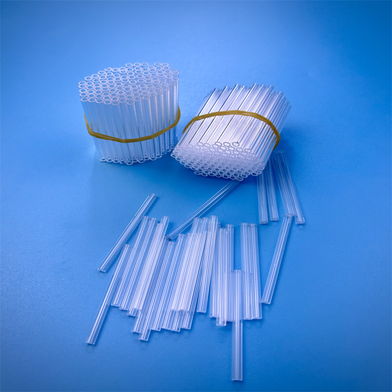
Quartz substrates and hollow tubes are packed using high-density tailored EPE foam cavities, dust-free electrostatic protective films, and hermetic vacuum foil sealing. Finished packs are placed inside reinforced, fumigation-free wooden export crates rated for heavy multi-tier stacking, complete with shockwatch and tilt-indicator sensors.
Request an Instant Engineering Review & Quote
Submit your CAD models (DWG, STEP, PDF) or tailored technical datasheets. Our factory engineers evaluate tolerances, material purity, and turnaround within 2 hours.