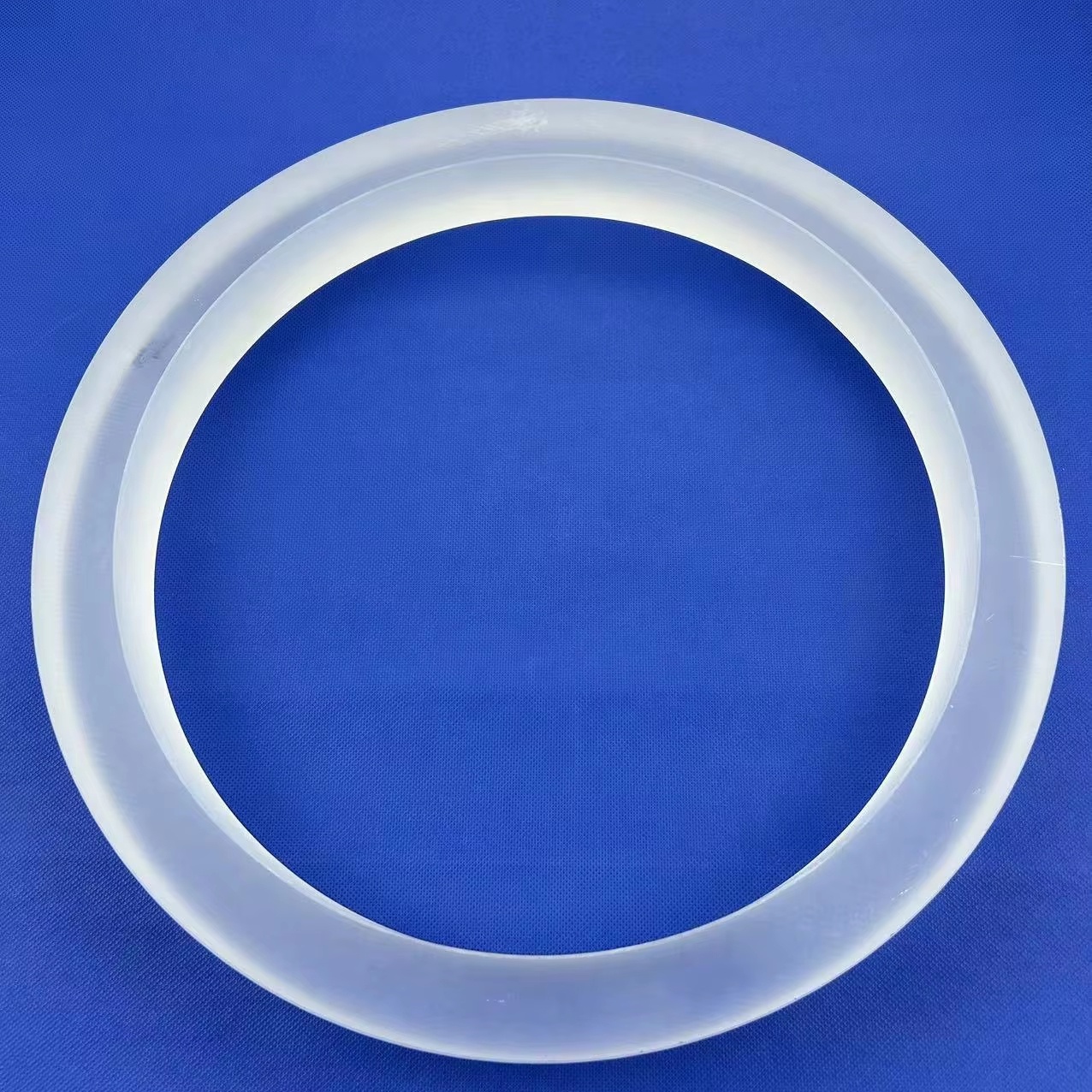
Factory Direct Catalog
Precision High-Purity Fused Quartz Components
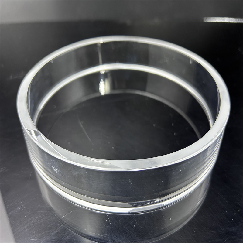
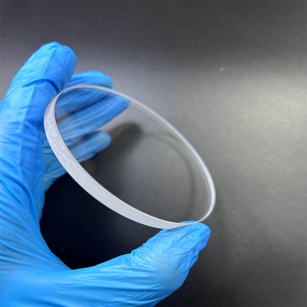
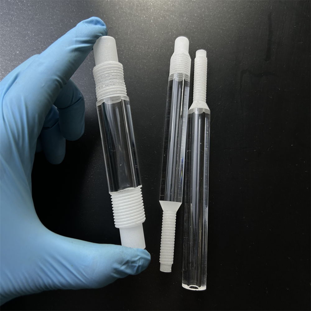
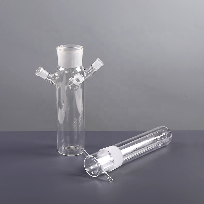
Manufactured under rigorous ISO dimensional controls at our Donghai production complex, our OEM/ODM custom quartz products serve critical functional roles across semiconductor CVD processing, UV optics, chemical synthesis, and cleanroom labware.

Material Science Matrix
Fused Quartz vs. Fused Silica: Engineering Grade Classifications
Procuring quartz components for critical environments demands precision alignment between hydroxyl content [OH-], bubble classes, and optical spectral windows. Evaluate standard industrial substrates across our processing capabilities:
| Substrate Grade | Spectral Range | Hydroxyl [OH-] Content | Primary Industrial Use-Case | Key Mechanical / Thermal Metric |
|---|---|---|---|---|
| JGS1 (Synthetic Silica) | 185 nm – 2500 nm (Deep UV) | < 5 ppm to 1200 ppm (Grade dep.) | Excimer laser optics, semiconductor photolithography, UV reactor tubes | Coefficient of Thermal Expansion: 5.5 × 10⁻⁷/°C |
| JGS2 (Fused Quartz) | 220 nm – 2500 nm (UV-VIS) | < 30 ppm | High-temperature viewports, furnace sight glasses, semiconductor carriers | Continuous thermal threshold: ~1100°C; Softening: 1683°C |
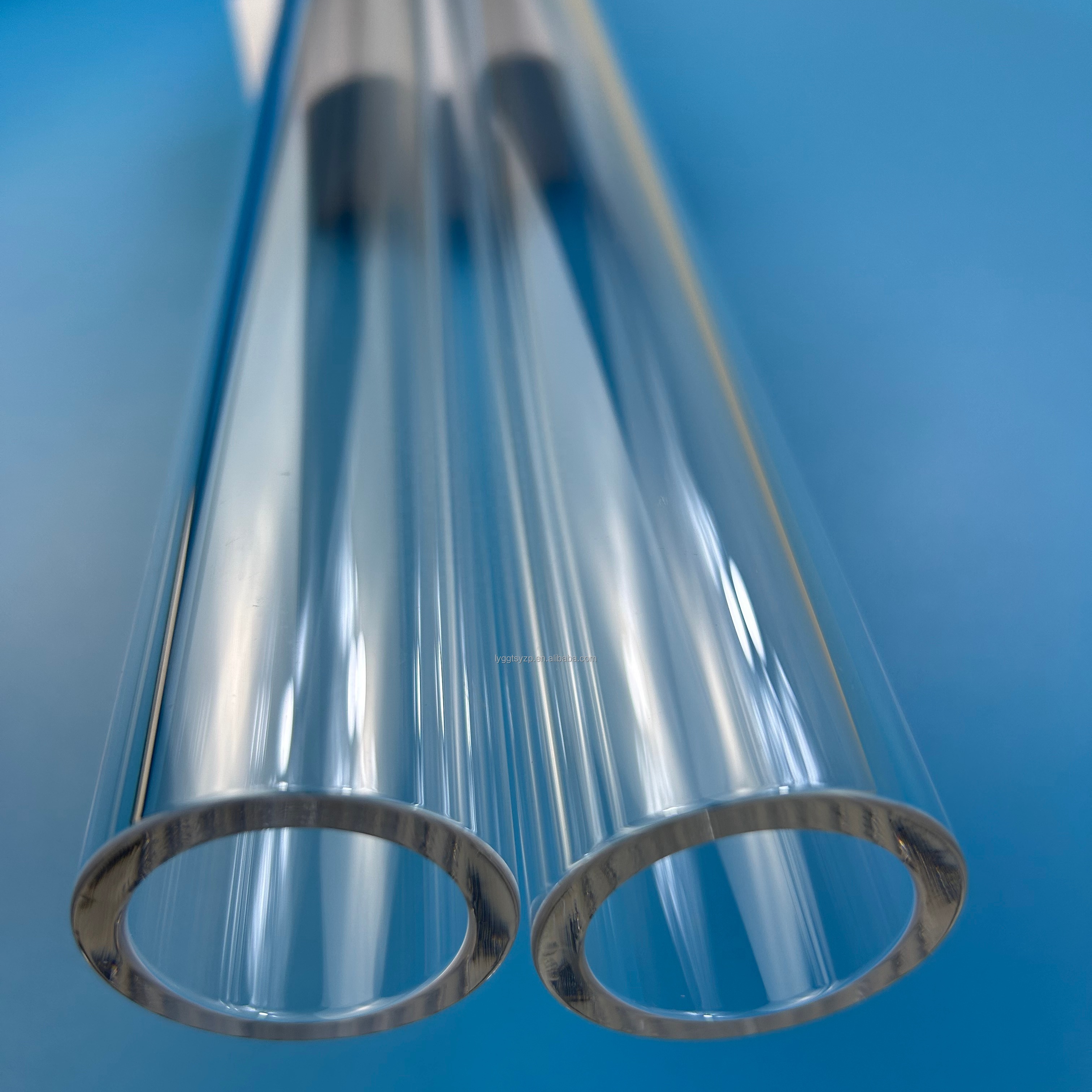
| JGS3 (Infrared Silica) | 260 nm – 3500 nm (Near-to-Far IR) | < 5 ppm (Water-free IR) | Infrared heating twin-tubes, pyrometry windows, gas chromatography | Absorption peak absent at 2.73 μm; High IR transmittance |
| Opaque Quartz (Quartz Foam) | Diffuse scattering | Standard | Thermal baffles, furnace insulation flanges, diffusion collars | Bulk density: 2.07 – 2.15 g/cm³; Enhanced thermal insulation |
Industry Foresight
Emerging Trends in Global Quartz Glass Sourcing
As semiconductor wafer diameters expand and wafer fabrication moves to sub-3nm nodes alongside hyper-efficiency solar cell technologies, fused quartz sourcing is undergoing significant technological shifts.
1. Sub-ppb Impurity Requirements
Next-generation Atomic Layer Deposition (ALD) and Extreme Ultraviolet (EUV) lithography systems are mandating fused silica with trace metallic elements (Fe, Cu, Ni, Na) under 1 part per billion to prevent lattice contamination in advanced wafer nodes.
2. Micro-Crack-Free Laser Machining
Traditional mechanical diamond grinding generates subsurface micro-fractures that fail under sustained 1100°C thermal cycles. The shift to ultrafast picosecond/femtosecond laser cutting and internal laser grooving ensures edge integrity and prolongs consumable lifespans by >40%.
3. Large-Scale Integrated Geometries
With TOPCon and HJT solar cells adopting M10/M12 large-format silicon wafers, quartz furnace tubes exceed 400mm outside diameters. Demand has shifted from multi-piece joined tubing to monolithic large-diameter quartz extrusions with integrated welded flanges.
Donghai Quartz Hub
Why Tier-1 Engineers Partner with Zunex Quartz
Headquartered in Donghai County, China's central silica refining hub, Zunex Quartz Products Co., Ltd. couples geographic mineral purity advantages with certified high-precision fabrication.
Strict Drawing Fabrication (OEM/ODM)
Every STEP, DWG, or PDF drawing undergoes comprehensive DFM (Design for Manufacturability) analysis by our senior quartz forming engineers within 2 hours, validating thermal expansion, CNC tolerances, and wall thickness uniformity.
Proprietary Laser & Flame Machining
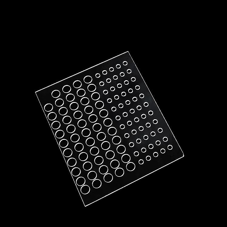
From fine micro-hole laser drilling (diameters down to 0.15mm) to complex five-axis CNC profile milling, precision fire polishing, and hydrogen-oxygen flame lathe welding, we manage cold and hot working in-house without outsourcing risk.
Export-Grade Vacuum Cushion Packaging
Exporting brittle quartzware globally requires specialized logistical engineering. We deploy triple-wall customized multi-density polyethylene (EPE) foam dampening housed in fumigation-free reinforced plywood cases to guarantee zero transit damage.
Procurement FAQs
Frequently Asked Questions on Custom Quartz Sourcing
Essential technical, commercial, and operational considerations addressed by our manufacturing engineering desk.
What engineering information is required to receive a definitive quotation?
To deliver an accurate fixed-price quotation within 2 hours, our team requires: (1) Dimensional drawings in 2D (PDF/DWG) showing dimensional tolerances and surface roughness requirements (Ra), (2) 3D CAD files (STEP/IGES) for complex milled geometries, (3) Material grade specifications (JGS1 UV, JGS2 Standard, or JGS3 IR), (4) Operating thermal and chemical parameters, and (5) Initial prototype batch quantity versus recurring production volumes.
How does fused quartz handle abrupt thermal shock compared to borosilicate glass?
Fused quartz features an extraordinarily low coefficient of thermal expansion (α = 5.5 × 10⁻⁷/°C between 20°C and 320°C), roughly 1/6th that of borosilicate 3.3 glass. This allows high-purity quartz components to be heated to 1150°C and plunged directly into cold water without macroscopic fracturing, making it irreplaceable for rapid thermal processing (RTP) and induction heating.
What are your standard machining tolerances for laser-drilled and CNC-ground plates?
For precision CNC optical cutting and grinding, standard manufacturing tolerances are held at ±0.05 mm, with high-precision CNC lapping achieving ±0.01 mm on planar thickness and parallelism under 3 arc seconds. Laser drilling processes achieve hole diameter tolerances down to ±0.02 mm with zero micro-cracking around borehole perimeters.
How do you certify material purity and internal optical inclusions?
All raw fused quartz batches originate from certified Donghai mineral refining streams with verified SiO₂ purity ≥ 99.99%. Every optical shipment can be accompanied upon request by Spectrophotometer UV-VIS-NIR transmission curves, cross-polarizer internal stress birefringence verification, and DIN ISO 10110 bubble/inclusion classification reports.
What is the average lead time for custom OEM quartz prototypes?
Standard stock dimensions (tubes and blanks) ship within 48 to 72 hours. Custom CNC machined, laser-drilled, or flame-formed prototypes typically complete fabrication, ultrasonic bath degreasing, cleanroom packing, and dimensional CMM inspection within 7 to 12 business days, with express air courier handling worldwide door-to-door.
Ready to Fabricate Your Custom Quartz Components?
Upload your STEP/DWG drawings or technical specifications. Our application engineers review all parameters and supply a formal DFM assessment and quotation within two hours.