Engineered Fused Quartz Substrates & Custom Fabrications
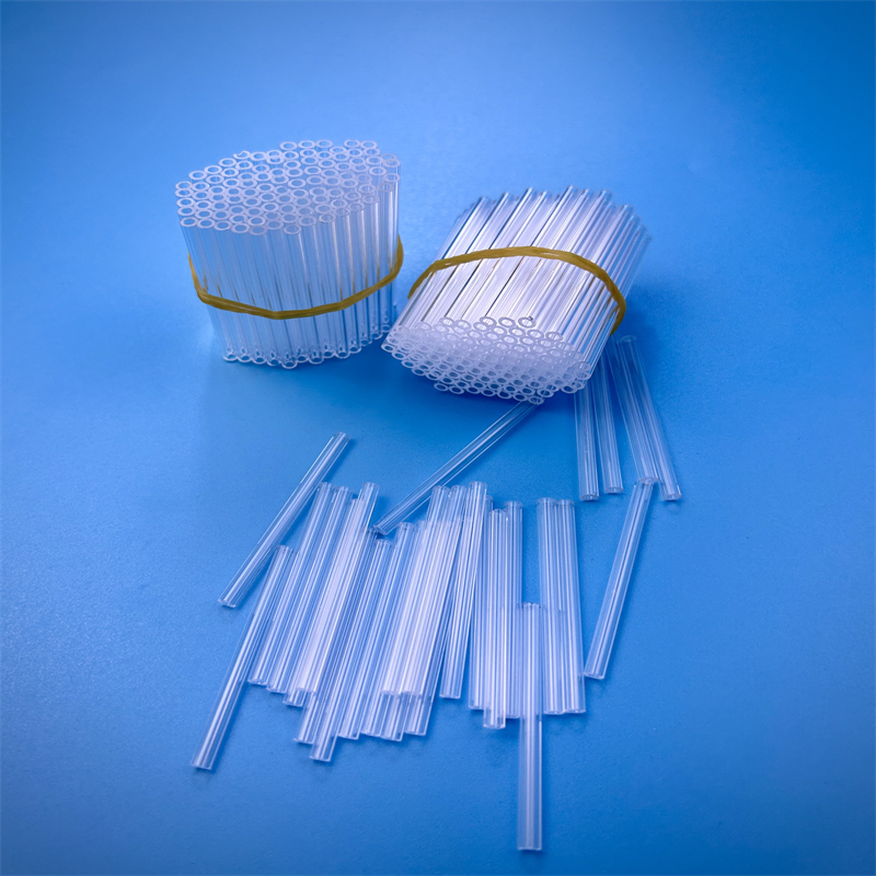
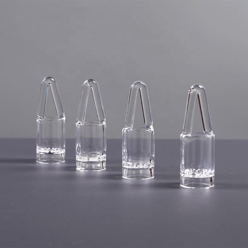
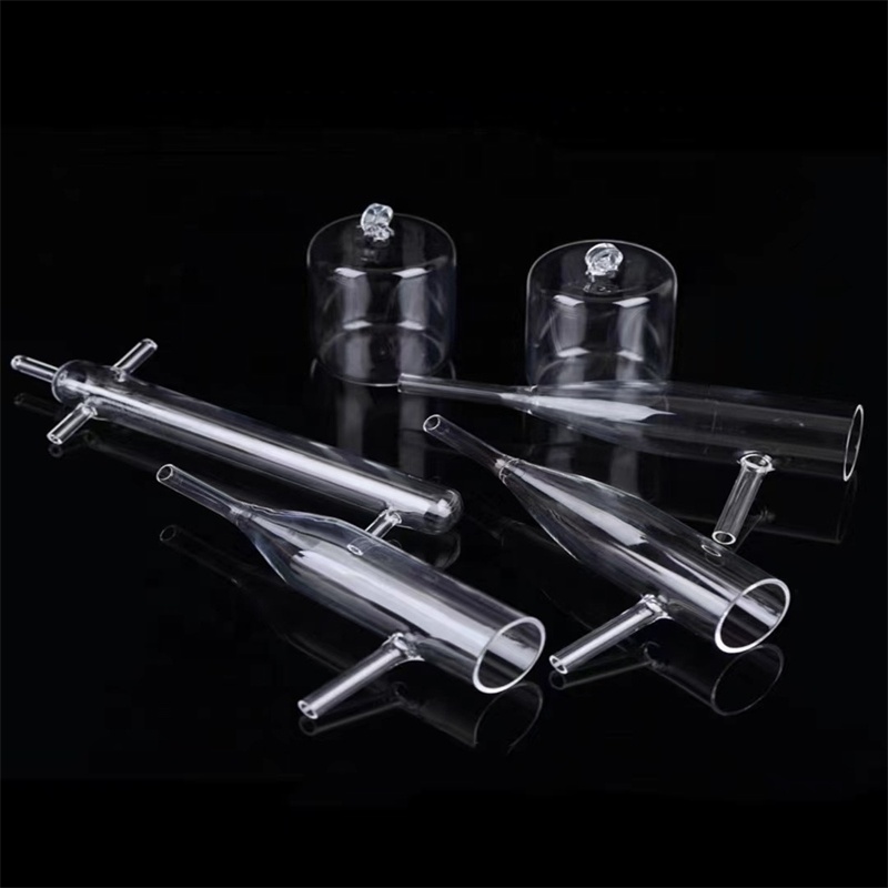
Direct manufacturer batch supply with laser precision grooving, optical micro-polishing, and CNC flame shaping to your exact CAD drawings.



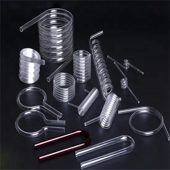
Material Science: Selecting Quartz Substrates for Critical Applications
A comprehensive engineering evaluation of synthetic fused silica vs. natural fused quartz substrates in advanced semiconductor, microfluidics, and photonics manufacturing.
JGS1 Synthetic Fused Silica
Synthesized via chemical vapor deposition of silicon halides. Offers exceptional deep-ultraviolet (DUV) transparency extending from 185 nm to 2500 nm, totally bubble-free structure, and almost zero trace metal impurities.
- Trace impurities: < 0.1 ppm
- Zero bubble class (DIN 58927)
- Excimer laser optics & lithography masks
JGS2 Optical Fused Quartz
Melted from purified natural crystalline silica under high-temperature vacuum. Ideal balance between thermal stability and optical transmission across 220 nm to 2500 nm.
- Trace elements: < 20 ppm
- Cost-effective optical windows & sight glasses
- High dielectric strength in RF plasma
JGS3 Infrared Grade Quartz
Vacuum-melted quartz subjected to specialized dehydration processing, driving hydroxyl (OH⁻) content below 5 ppm. Eliminates water absorption bands near 2.73 µm for broadband IR transmission.
- Extended transmission up to 3500 nm
- High thermal endurance (up to 1300°C)
- Pyrometry viewports & IR heat emitter casing
Physical & Dielectric Specifications Comparison
Verified physical values for design engineers choosing high-frequency and high-temperature quartz substrates.
| Performance Metric | JGS1 (Synthetic Silica) | JGS2 (Optical Quartz) | JGS3 (Dehydroxylated IR) | Borosilicate Float (Ref) |
|---|---|---|---|---|
| SiO₂ Purity Level | > 99.999% | ≥ 99.99% | ≥ 99.99% | ~ 81% |
| Coefficient of Thermal Expansion (CTE) | 5.5 × 10⁻⁷ /°C | 5.5 × 10⁻⁷ /°C | 5.5 × 10⁻⁷ /°C | 32.5 × 10⁻⁷ /°C |
| Max Safe Continuous Temp | 1150 °C | 1100 °C | 1150 °C | 500 °C |
| Dielectric Constant (1 MHz @ 25°C) | 3.75 | 3.78 | 3.80 | 4.60 |
| Dielectric Loss Factor (tan δ) | < 1.0 × 10⁻⁴ | < 3.0 × 10⁻⁴ | < 2.0 × 10⁻⁴ | 37 × 10⁻⁴ |
| Surface Roughness Achievable (Ra) | ≤ 0.3 nm (Super-polished) | ≤ 0.5 nm (Optical polish) | ≤ 0.8 nm (Standard polish) | ~ 1.5 nm |
Quartz Substrate Procurement Trends & Technology Roadmap (2025–2030)
How third-generation compound semiconductors (GaN, SiC), advanced packaging, and deep UV microfluidics are reshaping supplier benchmarks.
1. High-Frequency RF & Micro-Packaging
With 6G millimetric transceiver architectures requiring minimal dielectric loss tangent at frequencies past 110 GHz, quartz substrates are displacing traditional PTFE and alumina ceramics. Demand is accelerating for wafer thicknesses below 150 µm with tight Total Thickness Variation (<1 µm TTV).
2. Laser Induced Deep Etching (LIDE)
Traditional diamond micro-drilling creates micro-cracks and chip-outs along edge peripheries. Forward-thinking suppliers have transitioned to picosecond and femtosecond laser micromachining, achieving taper-free micro-via arrays (Through Quartz Vias - TQV) with pitch dimensions under 50 µm for next-gen interposers.
3. Supply Chain De-risking & Hub Sourcing
Procurement teams are shifting away from tiered distributors toward source manufacturers clustered in raw crystal industrial clusters like Donghai County. Direct engineering access reduces prototyping cycles from months to under 10 business days while guaranteeing raw material origin validation.
Enterprise Strengths: Why Tier-1 Engineers Choose Zunex
Combining Donghai's world-class quartz geology with CNC laser machining, strict cleanroom standards, and direct export certification.
Donghai Industrial Hub
Headquartered in China's Crystal Capital, giving us uninterrupted access to high-purity natural silica sources and reduced upstream procurement overhead.
Laser Finishing & Grooving
In-house precision laser drilling, ultrasonic milling, and CNC surface grinding to customer STEP/DWG drawings with tolerances down to ±0.02 mm.
Verified Rapid Response
Every RFQ is routed directly to a mechanical or optical engineer. We maintain a 100% verified response rate on international inquiries within ≤ 2 hours.
Damage-Proof Export Packaging
Custom multi-layer EPE foam suspension, moisture-sealed barrier films, and fumigated plywood cases tailored for delicate optical substrates shipped worldwide.
Frequently Asked Questions on Quartz Substrate Sourcing
Answers to critical engineering and commercial considerations encountered during qualification and volume ordering.
What are the key differences between quartz substrates and fused silica wafers?
What surface finish and flatness tolerances can be provided for custom quartz plates?
Can you produce complex shapes with through-holes, slots, and beveled edges?
What are the thermal limits and thermal shock considerations for fused quartz?
How does your engineering team review drawings, and what is the typical prototyping lead time?
Ready to Accelerate Your Substrate Sourcing?
Submit your custom specifications or mechanical drawings for immediate manufacturability review and a competitive direct-factory quotation from our Donghai engineering team.
Contact Us