
Engineered Fused Quartz & Silica Substrates
Explore our specialized portfolio of semiconductor-grade quartz disks, custom bell jars, precision tubing, and thermal apparatus ready for export delivery.
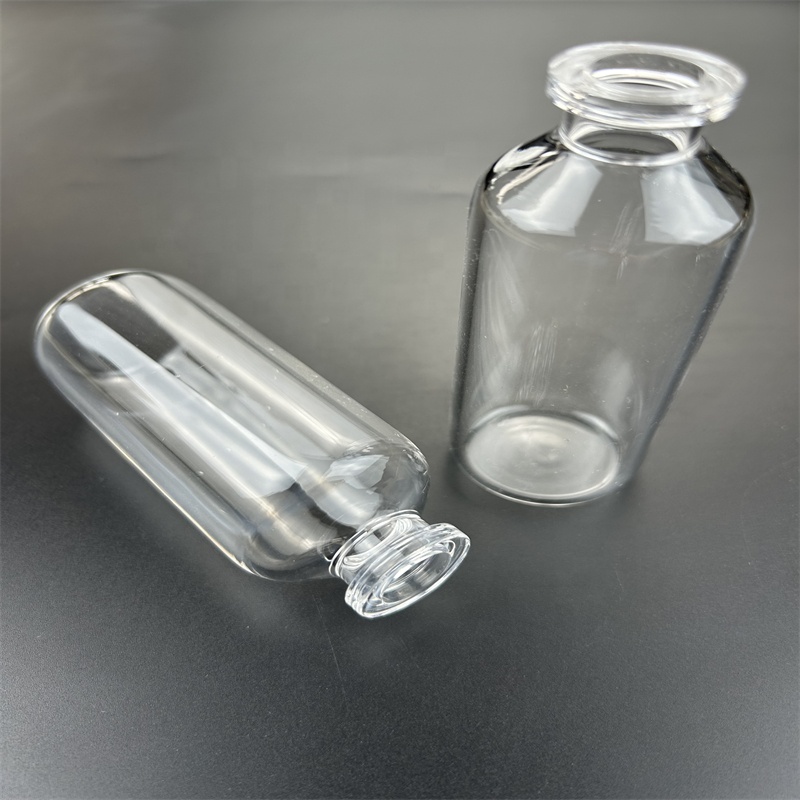
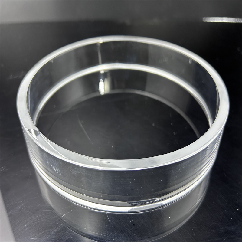
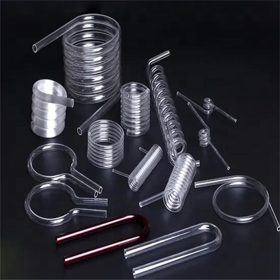
Laser ProfilingCustom Formed
Custom Different Sizes U-Bent Quartz Glass Spiral Tube with Moulding Cutting Bending and Welding Services

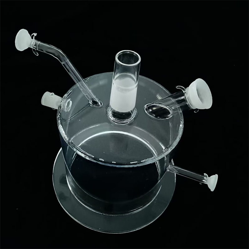
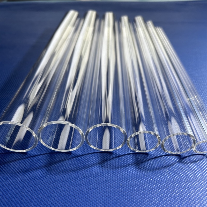
Boiler & ChemicalShock Resistant
Transparent High Pressure 99.99% Pure Quartz Glass Tube Furnace Boiler Chemical Applications Corrosion Bending Moulding
100%
Inquiry Response Rate
Verified Supplier Profile
≤ 2 Hours
Technical RFQ Feedback
Direct Engineer Review
43%
Repeat Buyer Ratio
Global Industrial Accounts
≥ 99.99%
Purity Grade Silicon Dioxide
Optical and Synthetic Classes
Engineering Whitepaper
Precision Substrate Science: Fused Silica vs. Quartz Wafers
Understanding structural, optical, and thermal behaviors under extreme microfabrication and high-frequency environments.
Synthetic Silica vs. Natural Quartz
Synthetic Fused Silica (JGS1) is synthesized from silicon tetrachloride (SiCl4) via vapor phase hydrolysis, eliminating metal element impurities down to parts-per-billion (ppb) scales. In contrast, fused quartz (JGS2) melted from natural crystalline rock delivers exceptional thermal stability at a cost profile tailored for bulk carrier trays, diffusion rings, and sight glass discs.
Thermal & Shock Resilience
Boasting a near-zero Coefficient of Thermal Expansion (CTE: 5.5 × 10⁻⁷ /°C from 20°C to 320°C), our substrates withstand instantaneous thermal gradients exceeding 1000°C without micro-fracturing. This parameter is decisive for plasma etch rings, microwave heating pedestals, and high-energy optical beam splitters.
Surface Planarity & Laser Milling
For microfluidics and semiconductor lithography carrier wafers, we apply chemical mechanical planarization (CMP) realizing Total Thickness Variation (TTV) under 2μm, Bow/Warp under 10μm, and surface roughness Ra < 0.5nm. Advanced ultrashort pulse laser micro-drilling ensures crack-free via channels without thermal debonding risks.
| Property Matrix | JGS1 (Synthetic Deep UV) | JGS2 (Optical Quartz) | JGS3 (Low-OH Infrared) |
|---|---|---|---|
| Transmission Window | 185 nm – 2500 nm (High UV cut-off) | 220 nm – 2500 nm (UV-VIS standard) | 260 nm – 3500 nm (Extended IR range) |
| Hydroxyl (OH⁻) Content | < 1200 ppm (High purity) | < 150 – 200 ppm | ≤ 5 ppm (Water-band peak suppressed) |
| Dielectric Constant (1 MHz) | 3.75 | 3.78 | 3.80 |
| Continuous Safe Temperature | 1100 °C | 1100 °C | 1150 °C |
| Primary Target Application | EUV/DUV Optics, Biochip Sensor Glass | Solar Cells, Sight Viewports, Quartz Tubes | IR Sensors, Pyrometer Ports, Heat Shields |
Regional Industrial Integration
Localized Applications for Enterprise Operations in David
Deploying specialized quartz wafer solutions to match regional agro-biotech labs, high-tech electronics fabrication, and logistics corridor initiatives.
Advanced Agricultural Biosensing & PCR
As David continues its emergence as a premier agro-tech and biomedical innovation center across Western Panama, our JGS1 quartz wafers serve as non-fluorescing, transparent microfluidic substrates for high-throughput DNA sequencing, seed pathogen scanning, and soil micro-nutrient spectroscopy devices.
Optical Quality Viewports for Logistics Hubs
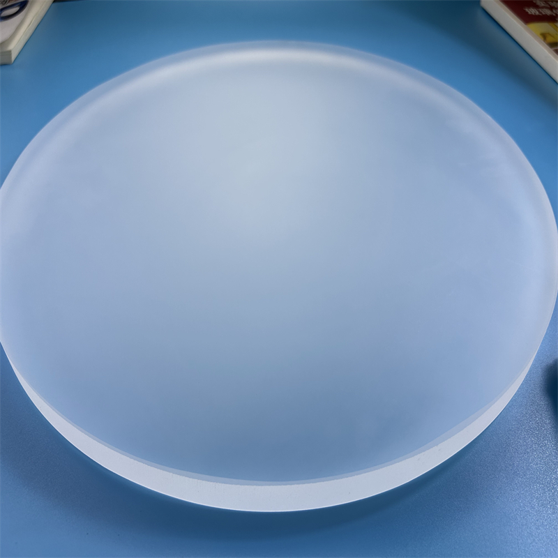
Serving regional marine logistics and industrial chemical parks operating through the Chiriquí transport corridor, our thick double-sided polished fused quartz sight glass discs operate reliably inside corrosive chemical treatment tanks, high-pressure autoclave valves, and maritime monitoring systems.
High-Efficiency Solar & Renewable R&D
Regional green energy pilot facilities and academic clean-tech testbeds in Chiriquí utilize our quartz wafers and tube components as high-durability carriers in photovoltaic cell doping, thin-film annealing, and concentrated solar power (CSP) thermal calibration runs.
Strategic Market Outlook
Emerging Procurement Trends in David & Chiriquí
Analyzing key structural shifts steering quartz component import, cold-chain medical instrumentation, and technical trade dynamics.
Transition Toward Precision Near-Net Substrates
Industrial procurement teams in David are steadily replacing standard raw quartz blanks with high-precision, CNC laser-grooved and edge-chamfered wafers. Procuring pre-milled, ready-to-mount components minimizes domestic scrap rates, decreases cleanroom assembly hours, and simplifies inventory control.
Supply Resiliency & Direct-to-Factory RFQ Channels
Given expanding freight connections via the Pacific shipping lanes and Tocumen cargo corridors, engineering firms in David prioritize direct partnerships with primary manufacturers in Donghai to bypass third-party trading markups, ensuring full trace certificates of raw silica purities.
Strict Adherence to Thermal Cycle Validation
Industrial autoclave operators and biomedical researchers locally require certified testing for thermal fatigue resistance. Procuring quartzware with verified annealing profiles guarantees zero structural delamination or micro-cracking across thousands of repeated heating-cooling shifts.
Manufacturing Excellence
Why Tier-1 Importers Trust Zunex Quartz
Direct heritage in China's quartz capital, comprehensive laser precision facilities, and verified global trade reliability.
Heart of China's Crystal Capital
Strategically situated in Donghai County, Jiangsu, Zunex draws upon deep mineral processing mastery and local synthetic raw materials, allowing seamless supply continuity for quartz plates, tubes, bell jars, and custom sapphire sheets at true factory-direct economics.
Advanced Laser Micro-Finishing Capabilities
We eliminate chip risks on thin quartz wafers using specialized laser cutting, precision hole drilling down to fractional millimeters, edge beveling, and slot grinding, ensuring flawless compatibility with complex micro-electro-mechanical systems (MEMS).
Engineered Customization to Print
Whether you require single customized prototypes or volume repeat production batches, our in-house engineering team audits your CAD/STEP drawings for processing tolerances, surface finishes (optical polish 80/50, 60/40, or frosted), and structural limits within two hours.
Procurement Clarity
Frequently Asked Questions by Buyers in David
Essential guidance covering packaging integrity, customs documentation, optical grading, and dimensional tolerances.
Can Zunex fabricate wafers precisely to custom engineering drawings?
Yes. Custom processing to drawing is our central competency. Simply share your CAD, STEP, or PDF drawing noting required diameter, thickness, flat or notch orientation, bevel edge profile, and acceptable surface defects. Our production engineers conduct a comprehensive manufacturability check before issuing guaranteed technical quotations.
How do we determine whether our application requires JGS1 or JGS2?
If your installation involves UV spectrometry, excimer laser windows, photolithography under 250nm, or deep ultraviolet sterilization lamps, JGS1 (Synthetic Silica) is essential to eliminate fluorescence and solarization losses. For standard visual observation ports, high-heat boiler tubes, or IR heating pedestals, JGS2 provides identical physical strength at optimized raw cost.
How are fragile quartz wafers packed to prevent breakage during transit to Panama?
We deploy certified export packaging: each wafer or optical disc is sealed in an anti-static cleanroom cassette or individual wafer tray, surrounded by thick high-density polyethylene shock foam, moisture-barrier wrapping, and securely encased in custom fumigated wooden crates designed to absorb multi-modal freight vibrations.
What typical thickness and diameter tolerances can be maintained?
Standard CNC grinding tolerances achieve ±0.05 mm on diameter and ±0.02 mm on thickness. For specialized semiconductor-grade and MEMS carrier wafers, double-sided optical lapping achieves thickness tolerances down to ±0.005 mm, with parallelism under 5 arcseconds and surface scratch-dig ratings conforming to MIL-PRF-13830B.
What is your typical production turnaround and quote response time?
Our verified response rate is 100%, with technical quotes delivered within 2 hours. Prototype wafer batches typically ship within 7 to 10 working days upon drawing freeze, while standard quartz tubes, rods, and regular polished discs are often ready for immediate dispatch via DHL, FedEx, air cargo, or ocean consolidations.
Ready to Expedite Your Custom Quartz Substrate Order?
Submit your CAD files, technical dimensions, or target application specs. Our engineering specialists are online to evaluate tolerances and provide instant direct-factory pricing.
Send an Inquiry