Export-Grade Quartz & Fused Silica Substrates for Canadian R&D
From single-piece prototyping for quantum photonics labs to scalable runs for cleanroom semiconductor processing, explore our verified optical, thermal, and chemical apparatus lines.
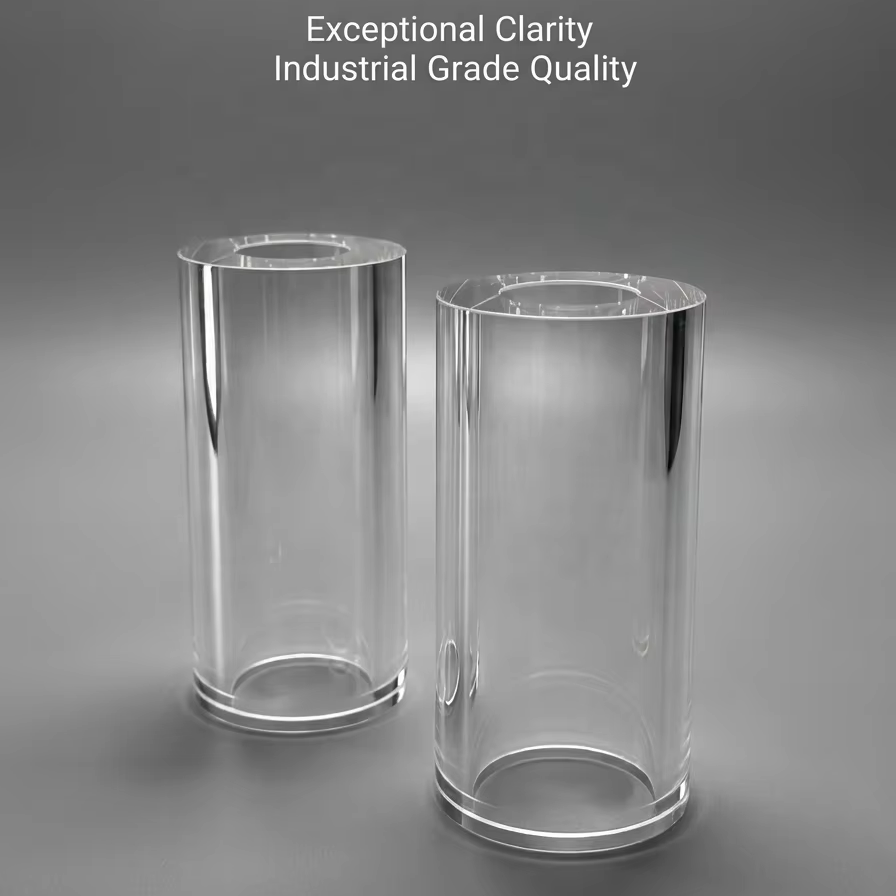
Factory Custom Both Ends Polished High Purity Transparent Quartz Twin Tube Bending Moulding Welding Cutting Capabilities
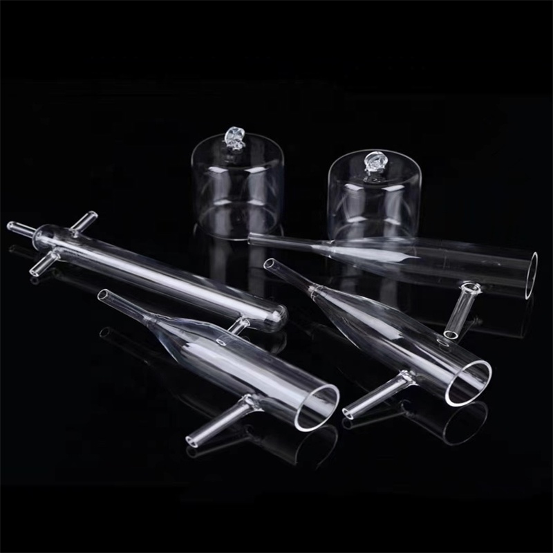
Custom Clear Laboratory High Temperature Twin Tube 99.99% Pure Quartz Glass Tube CVD Furnace Vacuum Bending Welding Services
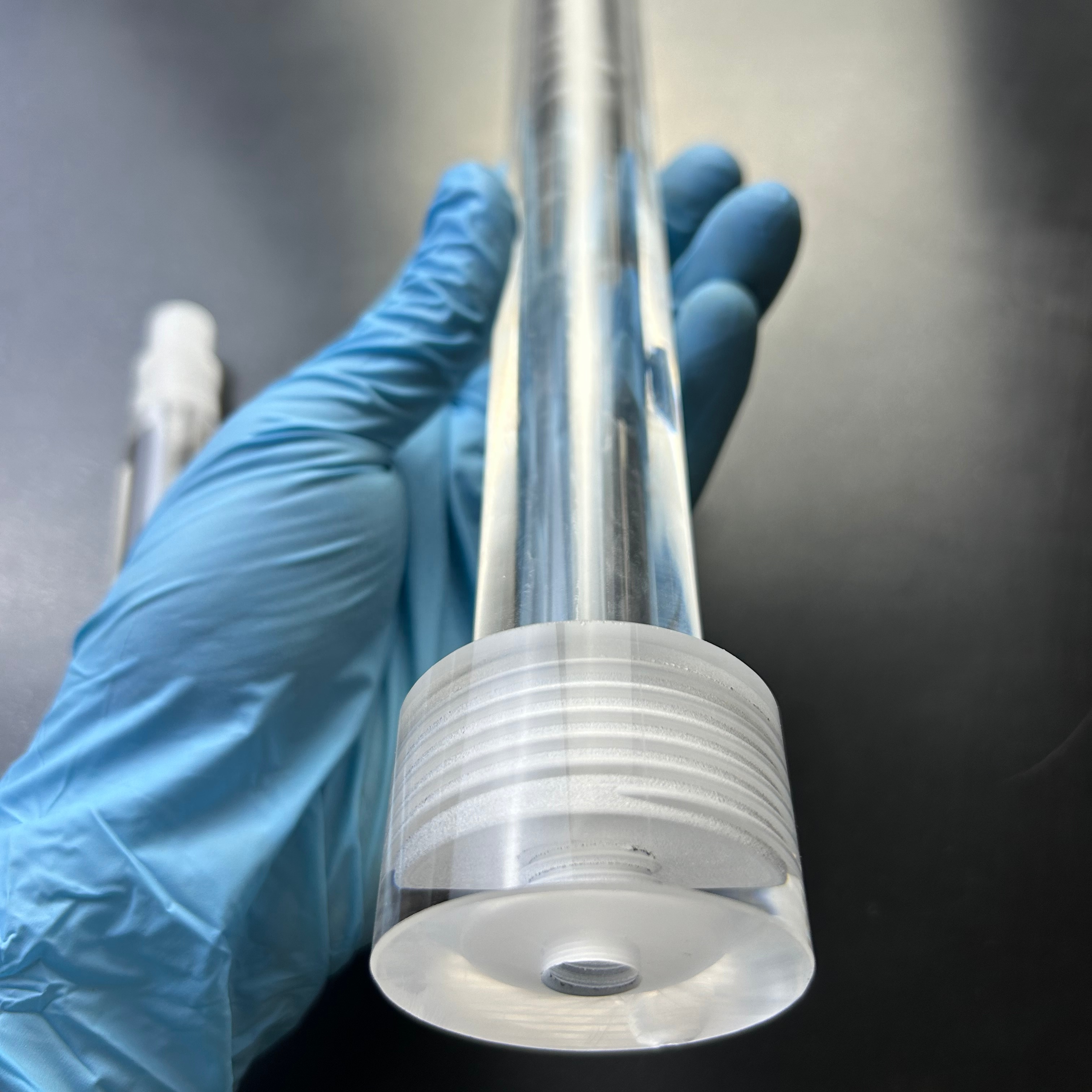
Customizable High Pressure High Quality Polished Clear Transparent 99.99% Pure Quartz Glass Twin Tube Bending/Welding/Cutting
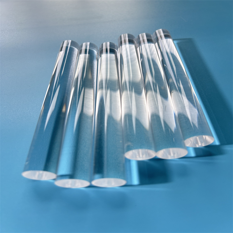
Custom Guitu Quartz GT Model High Purity Optical Quartz Light Guide Cylinder Rod 99.99% SiO2 for Optical/Semiconductor
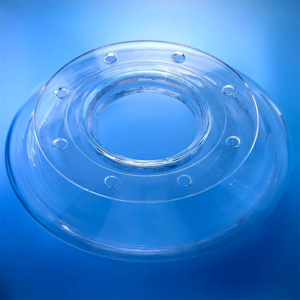
Customize Size Thickness Twin Tube Clear High Purity Flange Quartz Tube Fused Silica Polished Flange Ring Bending Welding
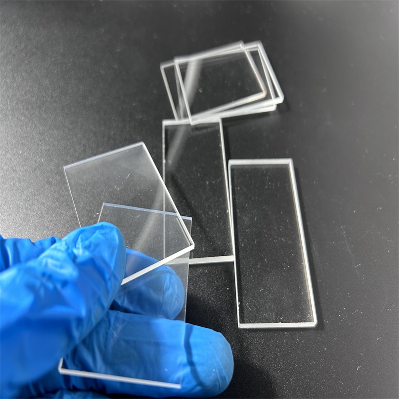
Customized High Temperature Transparent Fused Quartz Glass Sheet Welding Cutting Services Clear Plate Custom Sizes Optics Grade
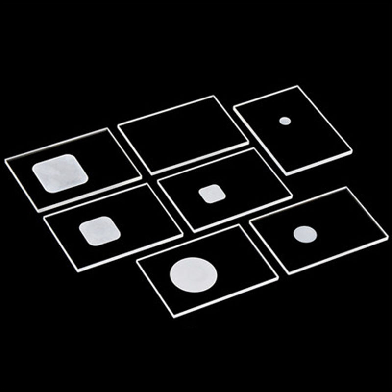
High Temperature Fused Quartz Glass Sheet for XRD Sample Tank Testing Chip Slotted Carrier Cutting Service Custom Sizes 1100C

Chemisorption BET Test High Pressure 99.99% Pure Ozone Free Clear Quartz Glass Twin Tube Bending Welding Services Quantachrome
Need Custom Drawing Tolerances or Instant CAD Quotation for Toronto Delivery?
Direct export pricing, full material certifications (RoHS, Reach, Purity Assay), and express door-to-door air freight to Pearson YYZ.
As advanced engineering clusters across the Greater Toronto Area (GTA)—stretching from the downtown Toronto MaRS Discovery District to the quantum, photonics, and semiconductor hubs in Markham, Mississauga, and Waterloo—accelerate their prototyping cycles, procurement managers face rigorous demands for ultra-flat, high-transmission fused silica substrates. Navigating thermal shock up to 1100°C, deep ultraviolet (DUV) laser transmission down to 185 nm, and near-zero coefficient of thermal expansion (CTE) requires engineering-led factory direct sourcing.
Selecting Substrate Material: Synthetic Fused Silica vs. Natural Fused Quartz
Choosing the exact glass grade governs spectral transmission cutoffs, laser-induced damage thresholds (LIDT), OH- radical absorption, and thermal deflection during thin-film deposition.
| Grade Standard | Synthesis Process | SiO₂ Purity | Transmission Window | Hydroxyl (OH⁻) Level | Primary Toronto / Ontario Applications |
|---|---|---|---|---|---|
| JGS1 (Corning 7980 / Suprasil Equivalent) | Synthetic vapor phase chemical deposition (SiCl₄ oxidation) | ≥ 99.999% | 185 nm – 2500 nm (Deep UV & Excimer) | High (> 800 – 1200 ppm) | DUV laser windows, quantum optical cavities, flow cells for biophotonics |
| JGS2 (Commercial Fused Quartz) | Oxy-hydrogen flame fusion of natural high-purity quartz crystal | ≥ 99.99% | 220 nm – 2500 nm (Near-UV to Visible) | Medium (approx. 150 – 200 ppm) | Industrial sight glasses, UV curing plates, standard lithography carriers |
| JGS3 (Infrasil Equivalent) | Electric vacuum fusion of natural quartz gravel (dry silica) | ≥ 99.995% | 260 nm – 3500 nm (Broadband & SWIR / MWIR) | Ultra-low (< 5 – 8 ppm, Water-Free) | IR spectroscopy windows, mid-wave IR sensors, laser pyrometer viewports |
| Semiconductor Diffusion Grade | Multi-stage purified electric arc fusion | ≥ 99.998% | Broadband furnace transmission | < 30 ppm | CVD/LPCVD process tubes, slotted wafer boats, epitaxial reaction chambers |
Unlike conventional borosilicate or soda-lime float glass, pure fused silica (SiO₂ ≥ 99.99%) features an exceptionally tightly knit amorphous silicon-oxygen tetrahedral framework. This molecular topology translates directly into an extremely low coefficient of thermal expansion of 5.5 × 10⁻⁷ /°C between 20°C and 320°C. For Toronto precision instrument designers, this allows substrates to endure abrupt temperature swings exceeding 1000°C into ice water quenching without microscopic fracture propagation.
Fused Silica Substrate Applications Across the Greater Toronto Tech Corridor
How leading universities, private R&D consortia, and defense manufacturers deploy Zunex custom quartzware throughout Southern Ontario.
1. Quantum Optics & Nanophotonics (Toronto-Waterloo Triangle)
Southern Ontario represents one of the world's dense clusters for quantum communication, quantum cryptography, and trapped-ion computing architectures.
- λ/10 surface wave-front flatness for ultra-low phase distortion optical setups.
- Laser-damaged threshold testing with surface roughness Ra < 0.5 nm (super-polish).
- Dual-side anti-reflective (AR) coated JGS1 synthetic silica viewports.
2. Biomedical Microfluidics & Diagnostics (MaRS Discovery District)
Toronto's medical discoveries rely on ultra-clean optical windows for multi-spectral fluorescence microscopy, DNA sequencer chips, and micro-capillary cytometers.
- Zero autofluorescence in DUV-NIR bands to maximize signal-to-noise ratio.
- Laser micro-machined microfluidic channels, CNC ultrasonic countersunk holes.
- Biocompatible, leach-free, heavy metal contamination under 0.1 ppm.
3. Semiconductor R&D & MEMS Wafer Carriers (Markham & Richmond Hill)
Cleanrooms and microelectronics test labs require high chemical resistance against violent wet-etch acids (HF, piranha) and high-temperature thermal annealing.
- 2-inch, 4-inch, 6-inch, and 8-inch fused silica dummy and process wafers.
- SEM-inspected wafer boats with micro-slot pitch accuracy down to ±0.05 mm.
- CVD furnace process tubes with ground flanges and quick-disconnect ports.
4. Aerospace, Defense & Satellites (Downsview & Mississauga)
Aerospace manufacturing across Peel and York regions relies on rugged viewports capable of handling severe pressure differentials and thermal stratifications.
- Extreme thermal gradient tolerance (ΔT > 1000°C) for atmospheric test beds.
- Custom pressure window stepped profiles with polished chamfered bevels.
- Mil-spec scratch-dig inspection certificates (MIL-PRF-13830B).
5. Advanced Analytical Labs & Catalysis Research (U of T & McMaster Corridor)
Material science departments across Ontario routinely perform high-temperature, high-pressure Chemisorption BET surface analysis and X-Ray Diffraction (XRD) crystal analysis. Our zero-background XRD sample plates and quartz twin-tubes withstand continuous reaction temperatures of 1100°C while resisting devitrification against corrosive volatile reactants.
- Compatible with standard Quantachrome, Micromeritics, and Rigaku XRD equipment without custom adaptors.
- Zero amorphous hump interference for sensitive powder XRD crystallography runs.
Southern Ontario Substrate Sourcing Trends (2025–2030)
Shifting trade channels, lead-time compression, and technical requirements affecting Canadian engineering purchasing agents.
Supply Chain Diversification from US Intermediaries
Toronto engineering firms historically paid up to 300% markup to US distributors who re-packaged Asian quartz blanks. By establishing factory-direct links with primary Donghai manufacturers, Canadian buyers capture wholesale OEM pricing, verify origin pedigrees, and eliminate transit bottlenecking through US customs ports.
Demand Surge for Laser Machining vs. CNC Milling
Traditional mechanical diamond drilling introduces sub-surface micro-cracks in fused silica, causing catastrophic fracture under cryogenic conditions or high laser fluences. Toronto photonics innovators are moving to non-contact CO₂ and femtosecond laser drilling and trepanning, cutting edge chipping below 20 microns.
Strict Compliance with CAD/STEP Direct Sourcing
Prototypes are rarely catalog-standard. Engineering universities across Southern Ontario require direct manufacturability reviews from native 3D CAD files (.STEP, .IGS, DWG) with tolerances specified down to ±0.01 mm, combined with comprehensive CMM (Coordinate Measuring Machine) inspection reports on arrival.
Factory-Direct Quartz Engineering: Raw Ingot to Precision Substrate
Based in Donghai County—the global epicenter of raw high-purity quartz reserves—Zunex Quartz combines primary melting with micron-level finishing.
Integrated Raw Material Reserve
Located directly in Donghai County, Jiangsu, we draw from direct natural crystal and high-purity synthetic precursor supplies. This guarantees uninterrupted availability of JGS1, JGS2, and JGS3 raw blanks even during global market crunches.
Full Spectrum Finishing Capabilities
Our workshop houses precision CNC slicing, planetary double-sided optical lapping, ultrasonic milling, flame welding, and cutting-edge industrial laser micro-drilling. We manufacture custom circular wafers, square windows, bevels, slots, and blind holes strictly to print.
Seamless Toronto DDP Air Logistics
Fragile quartzware demands exceptional packaging. Every component is ultrasonically cleaned, individually sealed in dust-free vacuum bags, nested in high-density custom-molded shock-absorbing EPE foam, and crated in export plywood cases for swift air clearance at Pearson (YYZ).
Frequently Asked Questions for Toronto Sourcing & Engineering Teams
Answers to common inquiries regarding lead times, logistics to Ontario, customs clearance, and manufacturing specifications.
What are typical transit times and shipping terms (Incoterms) for delivery to Toronto, Ontario?
How do you guarantee that optical substrates will not fracture during transit to Canada?
Can Zunex manufacture custom shapes, holes, and polished edges directly from our CAD files?
What inspection documentation and material traceability do you provide with our shipment?
Do you accept small-volume prototype orders from Canadian university research labs?
Accelerate Your Toronto Precision Optics or Semiconductor Project
Connect directly with Zunex engineers in Donghai. Send your PDF/STEP drawing, choose your grade (JGS1, JGS2, JGS3), and receive a verified manufacturability assessment with DDP Toronto freight pricing in less than two hours.