Precision Quartz Glass Tubes & Custom Optical Components
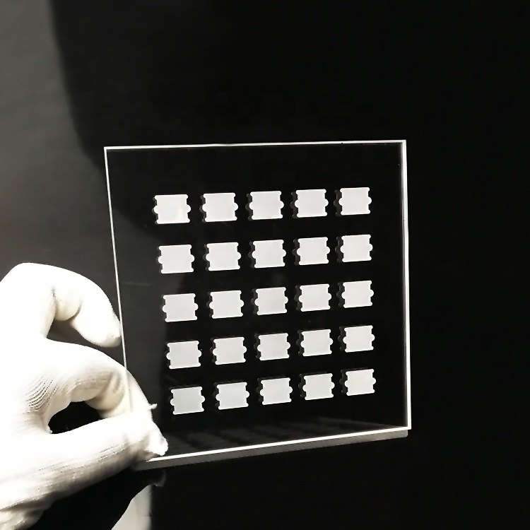
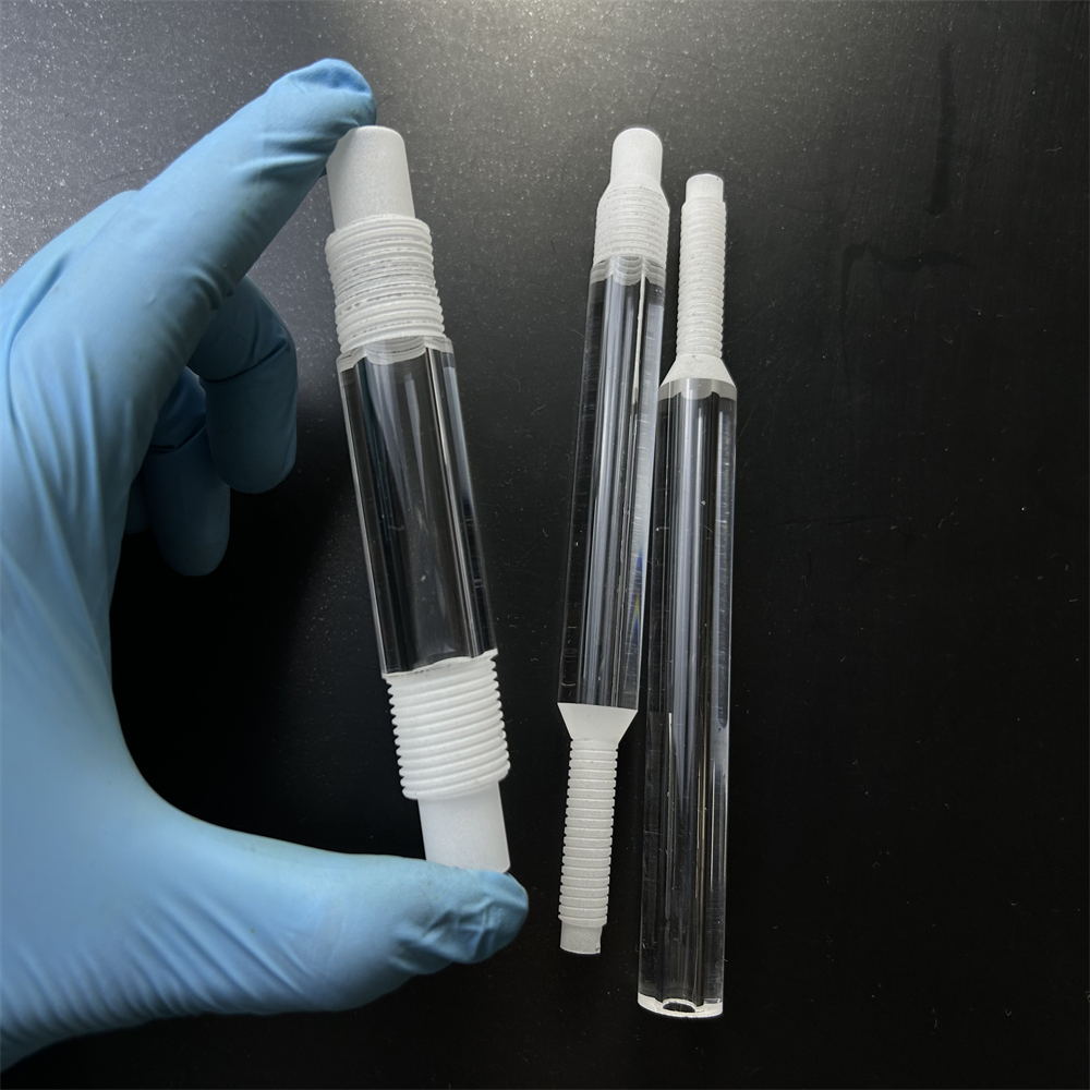
Direct OEM manufacturing with precision laser drilling, thermal bending, welding, slotting, and surface fire-polishing to your technical drawings.

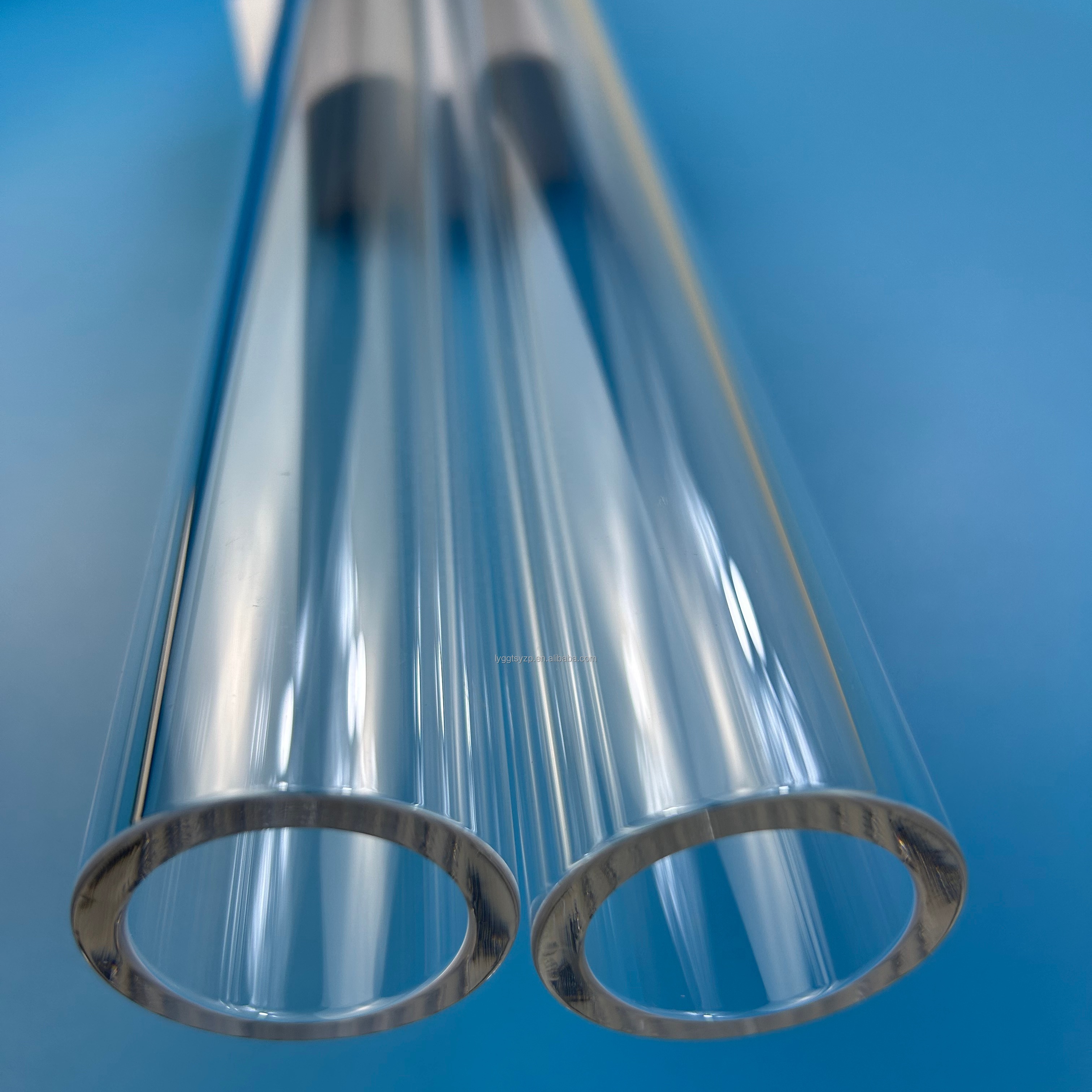
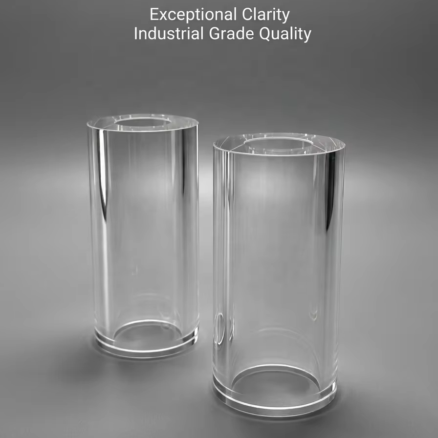

Silicon Valley Technical Context: Why Quartz Geometry Dictates Yield
Across the high-tech corridor of Santa Clara County, extending from North San Jose to Sunnyvale and Fremont, semiconductor fabrication facilities, rapid thermal processing (RTP) equipment builders, and photonics laboratories operate under strict yield metrics. Industrial quartz lamp tubes are fundamental thermal and photochemical barriers. Whether acting as envelope sleeves for high-intensity short-wave infrared (SWIR) emitters or housing excimer UV curing systems, raw material structural integrity governs process repeatability. Contamination traces of alkali metals (Na, K, Li) as low as 1 ppm lead to devitrification at 1000°C+, generating microscopic particulate shedding that can compromise nanoscale wafer fabrication. Zunex Quartz guarantees clean vacuum-electric fused silica with minimal OH concentration, customized for Silicon Valley's next-generation processing lines.
Localized Application Scenarios in the San Jose Innovation Corridor
How our custom quartz lamp tubes, twin-bore envelopes, and optical-grade fused silica serve critical hardware ecosystems throughout the South Bay.
Semiconductor Rapid Thermal Processing (RTP) & Epi Chambers
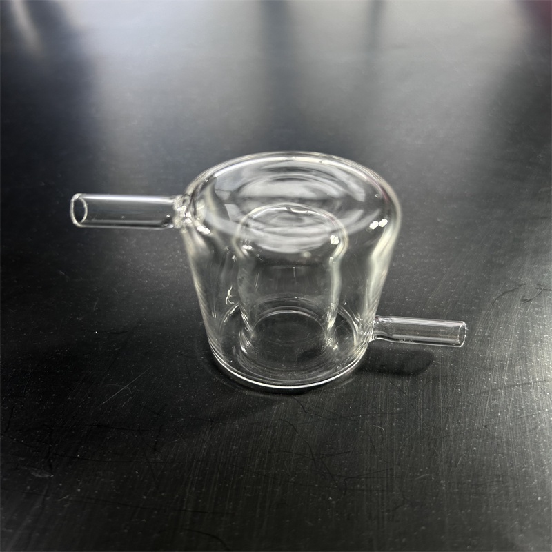
In North San Jose and Sunnyvale chip foundries, RTP, spike annealing, and epitaxial growth systems rely on high-output halogen quartz lamp arrays. Our dual-channel quartz twin tubes isolate heating filaments while providing superior broadband IR transmission (>92%) up to 3.5 μm without sagging under thermal ramp rates exceeding 150°C/s.
Extreme Ultraviolet (EUV) & Deep UV Lithography Subsystems
San Jose optical engineering firms develop high-power excimer laser systems and photochemical inspection tools. Utilizing synthetic grade JGS1 fused silica with near-zero bubble content and superior internal transmittance at 193 nm and 254 nm, our UV lamp tubes enable high photochemical dosage with zero ozone generation when required.
Advanced Solar Photovoltaic & Cleantech R&D
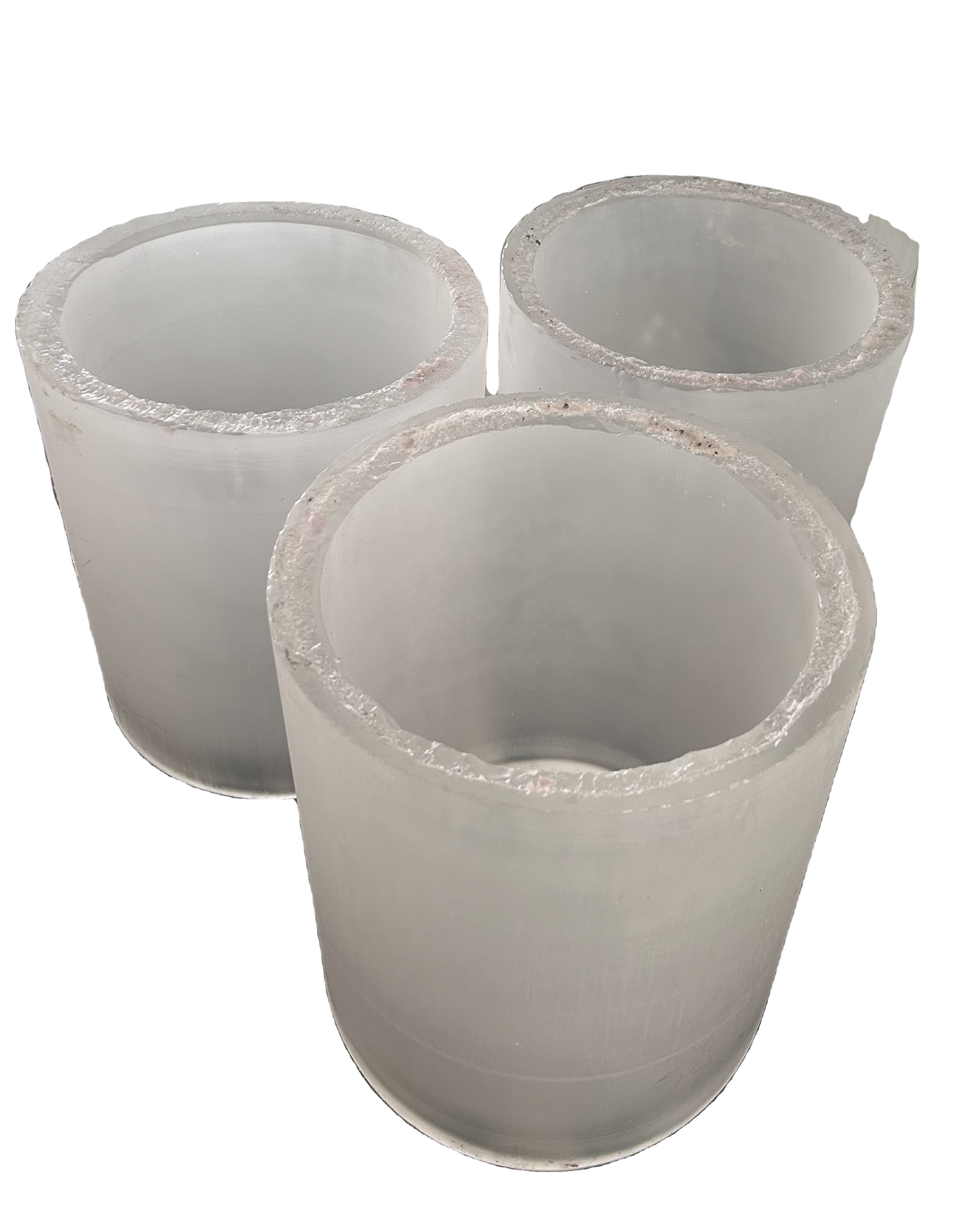
Serving clean-energy hubs in Milpitas and South San Jose, our large-diameter quartz process tubes and heating sleeves handle plasma-enhanced chemical vapor deposition (PECVD) and diffusion annealing. Their near-zero coefficient of thermal expansion (5.5 × 10⁻⁷/°C) ensures resilience against repeated high-speed thermal cycling.
| Technical Property | Synthetic Fused Silica (JGS1) | Optical Fused Quartz (JGS2) | Infrared Quartz (JGS3 / Low-OH) |
|---|---|---|---|
| Spectral Transmission Range | 185 nm – 2,500 nm (Deep UV) | 220 nm – 2,500 nm (UV-Vis) | 260 nm – 3,500 nm (Near-to-Mid IR) |
| SiO₂ Purity (Typical) | ≥ 99.999% | ≥ 99.99% | ≥ 99.98% |
| Hydroxyl (OH⁻) Content | < 1200 ppm (standard) / < 10 ppm (dry) | < 150 – 200 ppm | < 5 – 10 ppm (Water Peak Free) |
| Thermal Expansion Coeff. (0–300°C) | 5.4 × 10⁻⁷ K⁻¹ | 5.5 × 10⁻⁷ K⁻¹ | 5.5 × 10⁻⁷ K⁻¹ |
| Max Continuous Working Temp | 1100 °C | 1100 °C | 1150 °C |
| Typical San Jose Application | EUV optics, wafer inspection windows | Standard UV lamp sleeves, water reactor tubes | Semiconductor RTP emitters, IR soldering heaters |
Silicon Valley Thermal Processing & Quartz Sourcing Trends
How shifting semiconductor fabrication standards and advanced photonic hardware dynamics are reshaping technical procurement in Northern California.
Migration Toward Sub-2nm Semiconductor Thermal Nodes
As foundries transition to Gate-All-Around (GAA) nanosheet architectures, wafer processing budgets require sub-millisecond precision. Heating assemblies must minimize hydroxyl-driven light absorption. High-temperature emitter tubes require pure synthetic quartz shells with tightly controlled wall thicknesses (±0.05 mm) to avoid non-uniform hot spots across 300 mm substrates.
Demand for Direct-to-Fab Traceability & Cleanroom Packing
Hardware teams at Silicon Valley venture-backed startups and major OEMs reject unverified suppliers. Sourcing demands clear material certificates (GDMS impurity analysis) and cleanroom ultrasonic cleaning before vacuum bagging. This avoids costly in-house post-processing cycles prior to installation in ultra-high vacuum (UHV) systems.
Diversified Sourcing Direct from Raw Quartz Hubs
To reduce multi-tiered distributor markups and 16-to-24-week lead times from legacy US vendors, procurement directors in San Jose partner directly with integrated manufacturers based in Donghai County, China (the global hub for natural quartz mining and purification). This cuts direct procurement spend by 30% to 50% without sacrificing dimensional precision.
Enterprise Strengths: Engineering, Transparency & Direct Factory Value
Rooted in China's Crystal Capital (Donghai County, Jiangsu), Zunex Quartz combines primary raw material access with advanced micro-machining capabilities.
Precision Laser Finishing
Beyond traditional hot working, our facility operates multi-axis CO₂ and picosecond laser machining for micro-hole drilling, precision edge grooving, contour profiling, and crack-free tube slotting with clean kerf profiles.
Engineering Response Under 2 Hours
Technical RFQs submitted with CAD, STEP, or PDF drawings are reviewed directly by quartz fabrication engineers. We analyze manufacturability, thermal envelope stresses, and grade selection within 2 hours.
Silicon Valley Door-to-Door Logistics
Using custom multi-layer suspended foam packaging, vacuum-sealed PE sleeving, and reinforced plywood crates, we achieve a <0.2% transit damage rate via DHL, FedEx Priority, and air freight directly to San Jose (SJC/SFO).
Verified Third-Party Reliability
Maintaining a 100% verified response score and a 43% buyer repeat-order rate on Alibaba.com, Zunex provides complete trade transaction records, third-party credit audits, and batch-level dimensional inspection reports.
Frequently Asked Questions by San Jose Buyers
Direct technical and logistical answers regarding tolerances, material testing, shipping, and custom fabrication.