Featured Quartz Components & Substrates
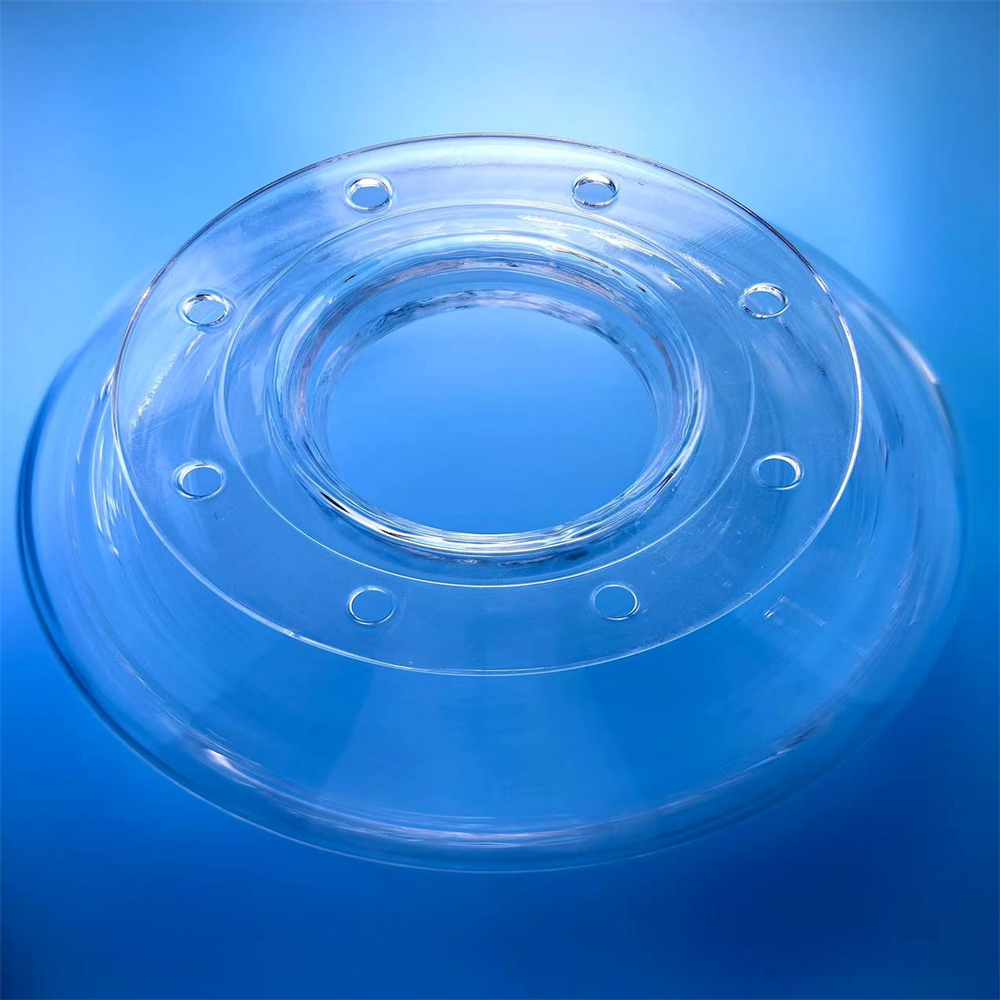
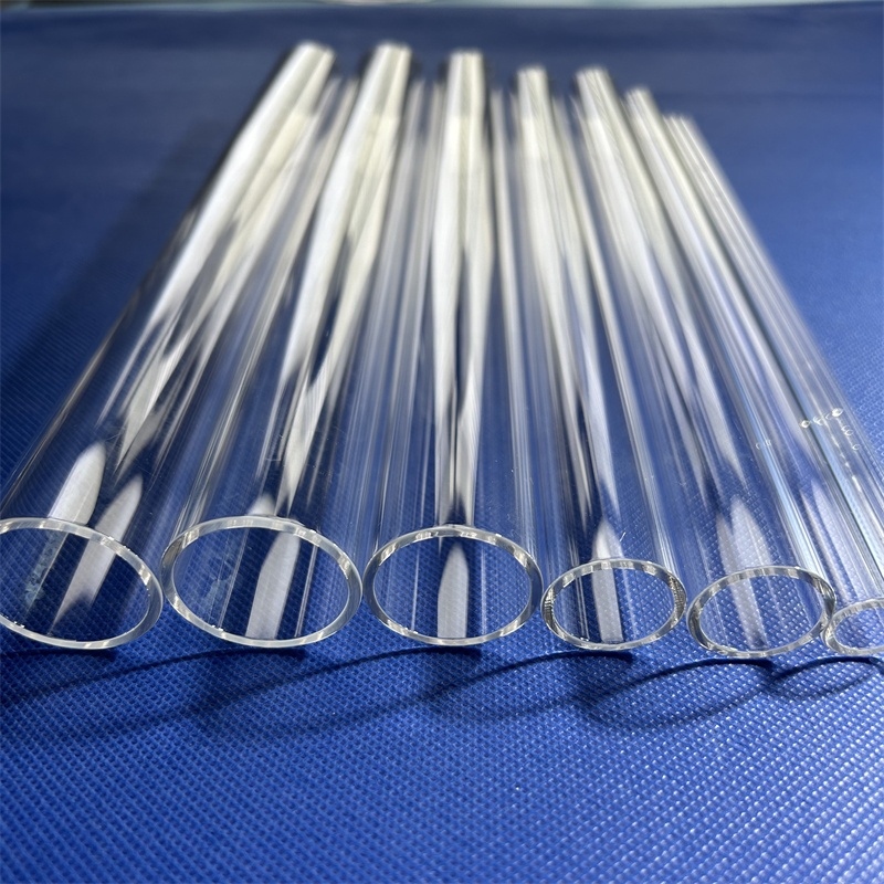
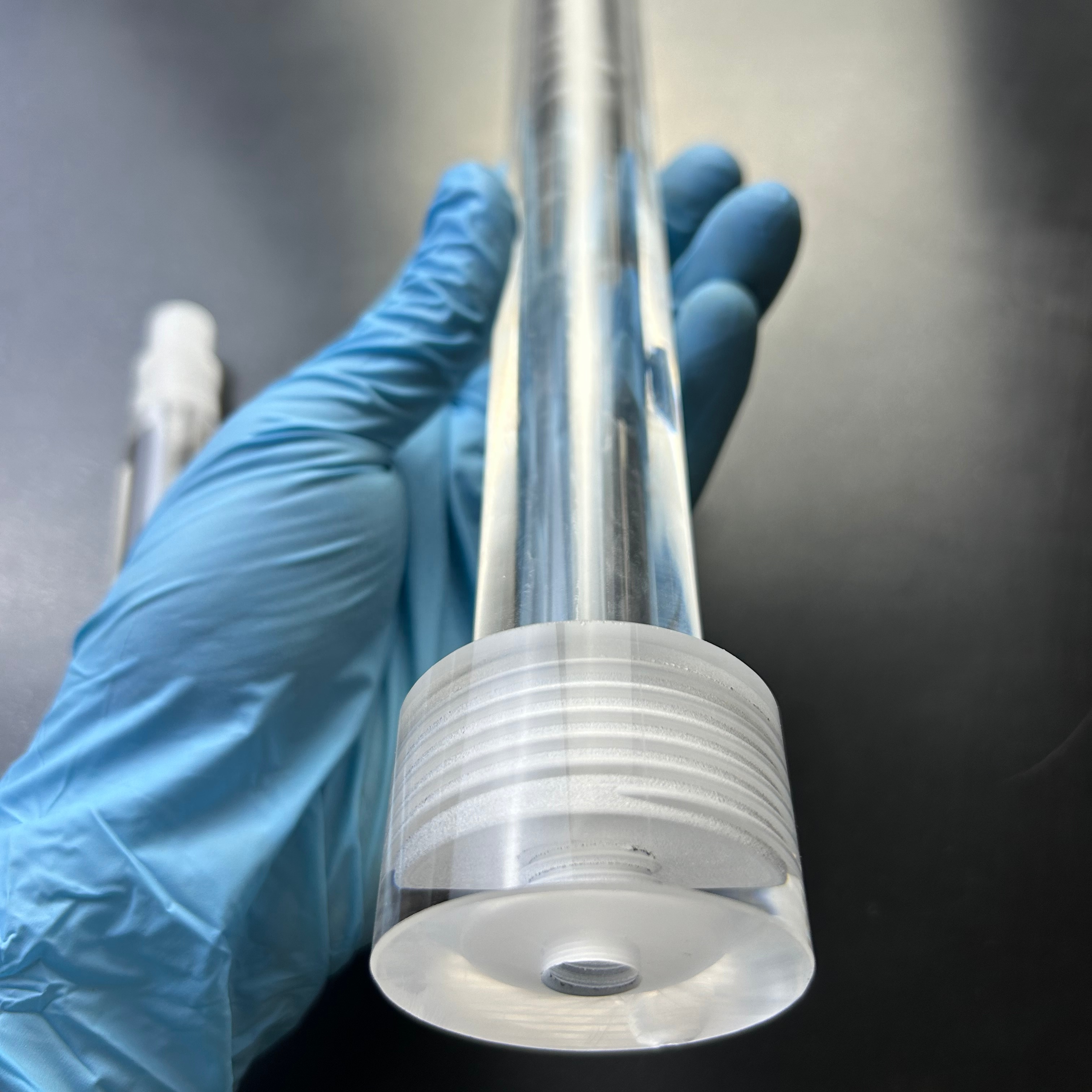
Directly supplied from our specialized quartz fabrication facility, delivering optical-grade quartz wafers, high-temperature furnace tubes, and precision-drilled plates meeting Japanese Industrial Standards (JIS).

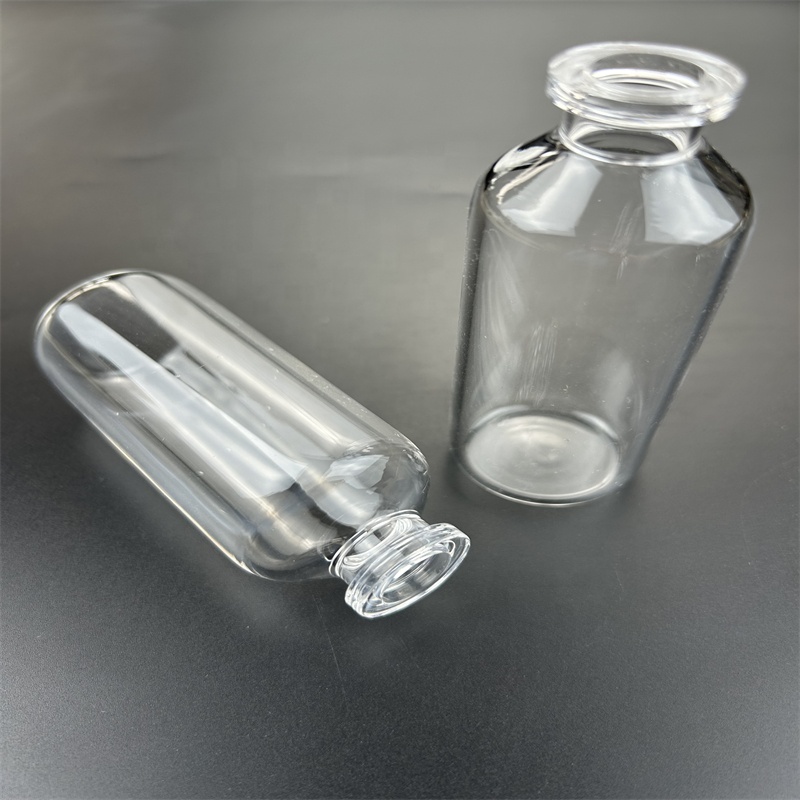
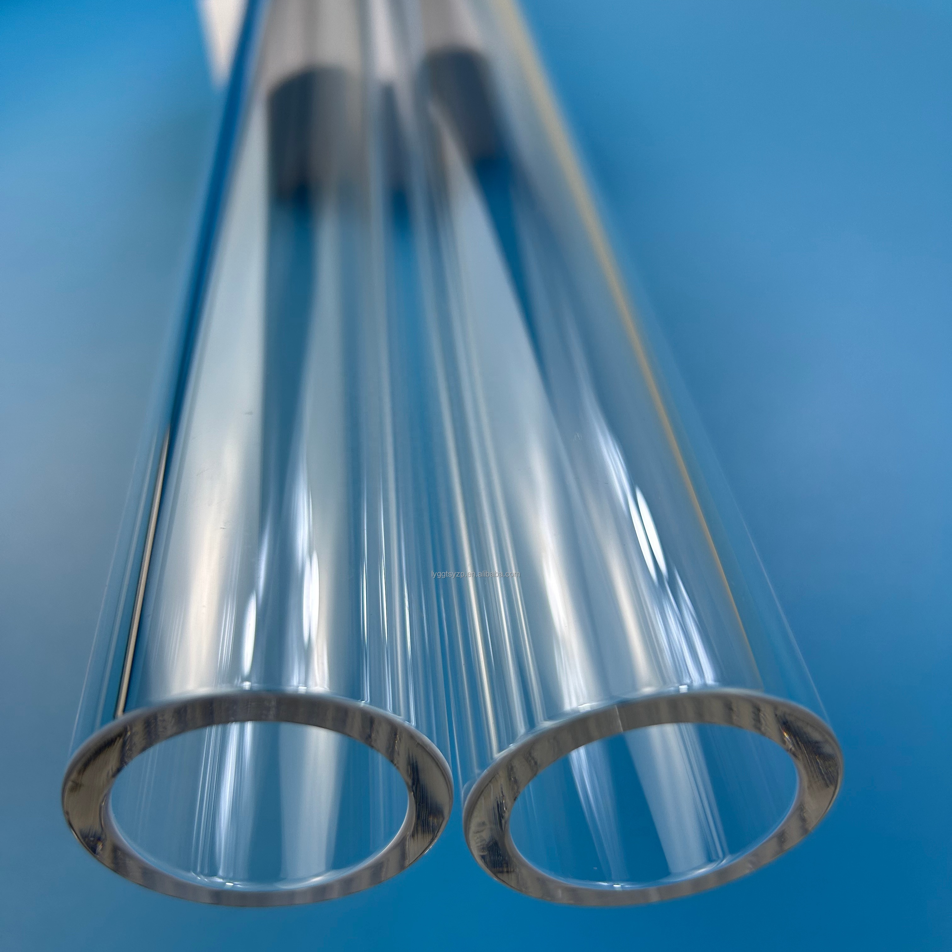
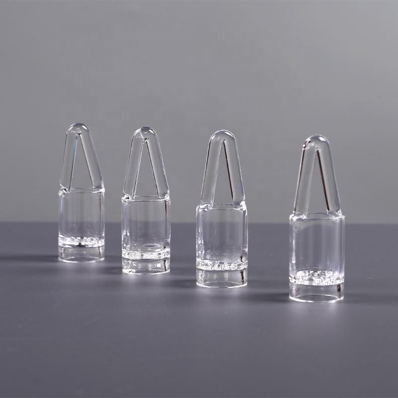
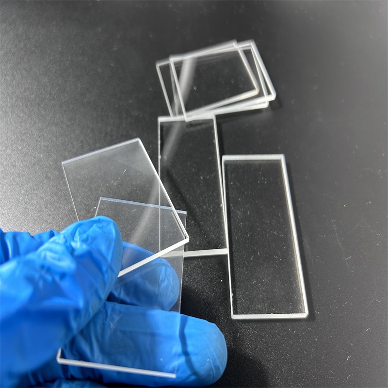
Precision Quartz Wafers & Synthetic Fused Silica: Empowering Chubu’s Industrial Architecture
As the economic powerhouse of central Japan, the Greater Nagoya area (spanning Aichi, Gifu, and Mie prefectures) represents one of the world's most sophisticated manufacturing ecosystems. Known historically as the epicenter of automotive innovation, aerospace development, and precision machinery, the region has transitioned rapidly into next-generation power electronics (SiC/GaN), advanced robotics sensing, and automotive lidar fabrication.
In high-temperature semiconductor manufacturing, micro-electro-mechanical systems (MEMS), and deep UV/infrared sensor packaging, standard borosilicate or soda-lime glass substrates cannot withstand the extreme thermal stresses and chemical environments involved. High-purity fused silica and quartz wafers serve as the indispensable substrate of choice due to their near-zero thermal expansion coefficient (5.5 × 10⁻⁷ /°C), superior optical transmission from 185 nm to 3500 nm, and exceptional dielectric stability under high-frequency operation.
Information Gain Metric: Our synthetic fused silica (JGS1) and natural fused quartz (JGS2/JGS3) wafers feature Total Thickness Variation (TTV) < 2.0 μm, surface roughness Ra < 0.5 nm (Super-Polished), and low trace metal contamination (< 1.0 ppm total), directly supporting advanced microfabrication protocols in Nagoya cleanrooms.
Supplying the Nagoya industrial market demands adherence to rigorous quality frameworks. Procurement engineers across Toyota City, Kariya, and the Nagoya Port high-tech zones operate under tight Just-In-Time (JIT) production rhythms. Zunex Quartz bridges direct-to-factory pricing with strict Japanese Industrial Standard (JIS) mechanical compliance, ensuring prototype-to-volume scalability with absolute dimensional integrity.

Optical & Physical Grade Matrix for Nagoya Engineering Teams
Select the optimal fused quartz substrate based on optical transmission window, hydroxyl (OH⁻) content, and working temperatures.
| Material Grade | Primary Composition | Spectral Transmission | Hydroxyl (OH⁻) Content | Key Chubu / Nagoya Applications |
|---|---|---|---|---|
| JGS1 (Synthetic Fused Silica) | Synthetic SiCl₄ (High Purity ≥ 99.999%) | 185 nm – 2,500 nm (Deep UV to Near IR) | ≤ 1200 ppm (Bubble Free Class 0) | Photolithography masks, UV laser windows, excimer laser optics, semiconductor inspection viewports. |
| JGS2 (Optical Fused Quartz) | Natural Crystal Quartz (≥ 99.99%) | 220 nm – 2,500 nm (UV to Visible Spectrum) | ≤ 150 – 200 ppm | Automotive sensor windows, industrial sight glasses, wafer carrier plates, solar cell diffusion carriers. |
| JGS3 (Infrared Fused Quartz) | Electrically Fused Crystal (≥ 99.99%) | 260 nm – 3,500 nm (Near to Far Infrared) | ≤ 5 – 10 ppm (Water Free) | Automotive infrared pyrometry, IR heating twin tubes, thermal chamber inspection windows, laser cutting optics. |
| Semiconductor Fused Silica | Thermal SiO₂ Solid Ingot | Broadband Standard | ≤ 30 ppm | Diffusion tube furnaces, quartz boats, LPCVD/PECVD bell jars, plasma etch ring components. |
Localized Quartz Applications in the Chubu Industrial Corridor
Customizing precision glass components to resolve engineering bottlenecks in Aichi's leading industrial sectors.
Automotive Sensor & LiDAR Packaging
Aichi Prefecture leads the globe in autonomous driving architectures. We engineer optical quartz cover windows, micro-prism blanks, and high-transmittance double-side polished JGS1 plates that protect vehicle sensors from stone chipping, thermal shocks (-40°C to 125°C), and environmental degradation.
SiC & GaN Power Semiconductor Epitaxy
In the transition toward 800V EV architectures, local Nagoya chipmakers demand quartz reaction chambers, injector nozzles, and high-purity carrier trays. Our 99.99% SiO₂ tooling ensures thermal integrity during epitaxial growth reaching up to 1300°C without metal ion leaching.
Aerospace Composite Thermal Processing
Serving the aerospace manufacturing hub around Central Japan International Airport (Centrair), we deliver specialized twin-tube infrared quartz heating emitters and quartz vacuum sight windows capable of enduring aggressive pressure differentials and composite curing cycles.
Precision Analytical & University Research
Collaborating with academic research facilities at Nagoya University and regional testing laboratories, Zunex provides microfluidic quartz chips, BET surface area analysis sample tubes, XRD zero-background sample holders, and custom optical quartz cuvettes.
EV Battery Thermal Management & Welding
During automated laser welding of prismatic lithium-ion battery terminals, high-energy laser spatter degrades standard optics quickly. Our custom fused quartz protective cover plates feature high laser damage thresholds (LDT) to extend optical maintenance cycles.
Direct OEM Custom Drawing Fabrication
Eliminate costly domestic multi-tier trading margins. We execute direct manufacturing according to customer CAD, DWG, and STEP files, supplying precision CNC milled steps, ultrasonic laser-drilled hole patterns, and chamfered edge profiles down to ±0.02 mm.

The Nagoya Quartz Supply Chain: Navigating Reshoring, Cost Pressures & Quality Control
Over the past three decades, procurement managers in Aichi and the surrounding Tokai industrial region relied almost exclusively on legacy domestic Japanese quartz fabricators. However, with surging cleanroom construction costs, expanding wide-bandgap semiconductor lines, and aggressive cost targets driven by global EV competition, Japanese purchasing teams are actively diversifying their supply lines.
Trend 1: Direct-from-Source Fabrication. By sourcing directly from Donghai County—the crystal and quartz capital representing over 70% of raw quartz processing capacity—Nagoya buyers reduce raw material procurement markups by 30% to 45% without sacrificing purity or optical class.
Trend 2: Laser Cold Finishing vs. Traditional Mechanical Slitting. Traditional quartz cutting generates micro-fractures along wafer edges, causing premature catastrophic failure during rapid thermal annealing (RTA) cycles. Our investment in advanced CO₂ and UV laser finishing delivers crack-free edges with minimum chipping (< 0.05 mm), ensuring reliable performance in thermal shock applications.
Trend 3: Transparent Traceability and Verification. Japanese engineering teams require verified proof of material purity, surface roughness, and lot consistency. Zunex Quartz provides full dimensional inspection reports, GD&T conformity certificates, and spectrophotometer transmission scans with each export consignment.
Why Engineering Teams Choose Zunex Quartz
Combining specialized quartz laser processing, high-volume raw material reserves, and engineering-driven customer service.
Rapid 2-Hour Response Time
Our verified response rate is 100% on international platforms, with an average turnaround under 2 hours. Your drawings and inquiries are reviewed immediately by dedicated quartz engineers, not generic sales agents.
Laser Drilling, Grooving & Cutting
Specializing in quartz laser micro-machining, we produce precise aperture holes, micro-channels, stepped discs, and complex notched wafer geometries with minimal HAZ (heat-affected zone) and no burrs.
Export-Safe Shockproof Packing
Quartz components are fragile. Every consignment dispatched to Nagoya Port or Chubu Centrair Airport is packed with custom-molded high-density PE foam, multi-layer vacuum bags, and reinforced export wooden crates.
Frequently Asked Questions for Nagoya Buyers
Clear technical and commercial answers addressing dimensional tolerance, customs clearance, and material authentication.
Ready to Discuss Your Quartz Wafer & Component Requirements?
Connect with our technical engineering desk serving the Greater Nagoya market. Upload your drawings or specification sheets for an expert feasibility review and a competitive direct factory quote within 2 hours.
Inquire Now