High-Purity Quartz Glass & Optical Substrates Portfolio
Engineered to satisfy stringent Japanese Industrial Standards (JIS R3204) and ISO Class 3 cleanroom handling requirements. High transmittance across deep UV (185nm) to mid-infrared (3500nm) spectrums.

Clear 99.99% Fused Quartz Twin Tube
Ozone-free welding, thermal resistance up to 1300°C, designed for rapid thermal processing (RTP) and selective infrared emitters.
Product Details →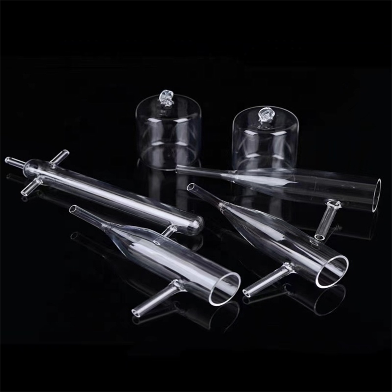
CVD Furnace High-Temp Quartz Twin Tube
Precision vacuum bending and fusion welding. Structural stability under high vacuum gradients in chemical vapor deposition processes.
Product Details →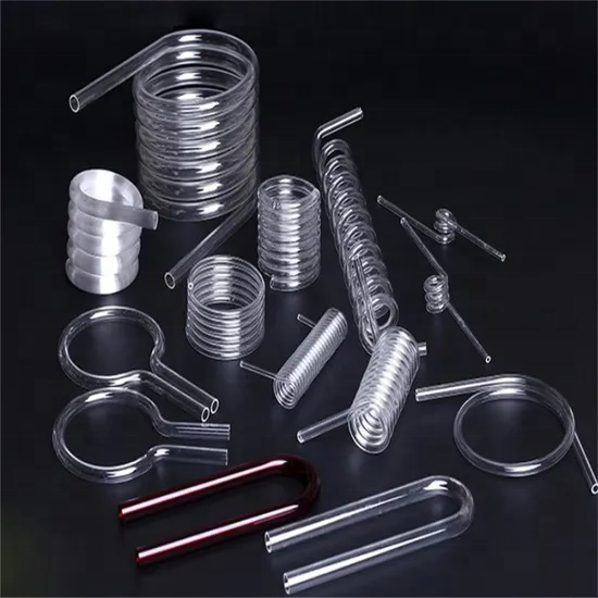
U-Bent Quartz Glass Spiral Tube
Accurate mechanical pitch moulding, cold laser cutting, and stress-relieved annealed joints for complex fluid heat exchangers.
Product Details →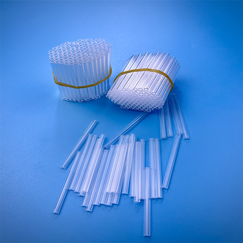
Optical Polished Transparent U-Bent Tube
Laser drilled, fire-polished, high OH-content or OH-free formulations engineered for photolytic sterilizers and spectroscopic sensors.
Product Details →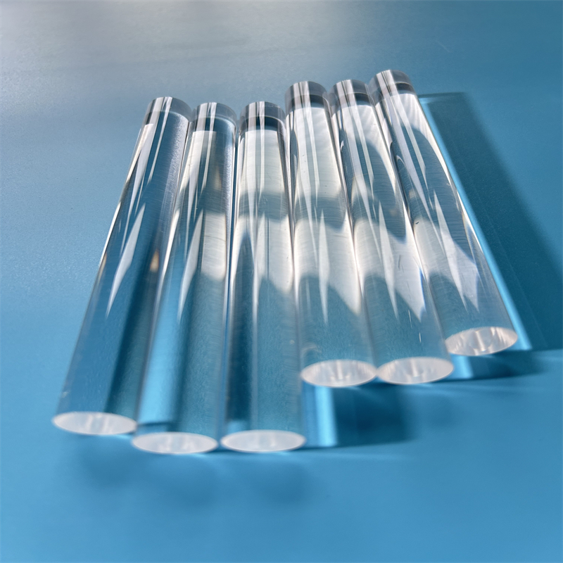
Optical Quartz Light Guide Cylinder Rod
JGS1 equivalent synthetic silica core with 99.999% purity. Optimized total internal reflection with minimal beam dispersion.
Product Details →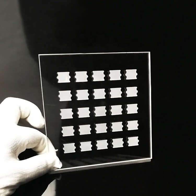
Circular Zero-Background XRD Sample Holder
Ultra-flat lapping (surface roughness Ra < 0.5nm). Zero diffuse scattering background tailored for crystalline diffractive analysis.
Product Details →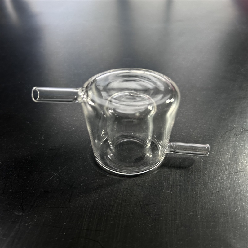
High-Purity Quartz Chemical Reactor Tube
Precision flange connections, chemical resistance against aggressive acids, optimized for high-temperature synthesis laboratories.
Product Details →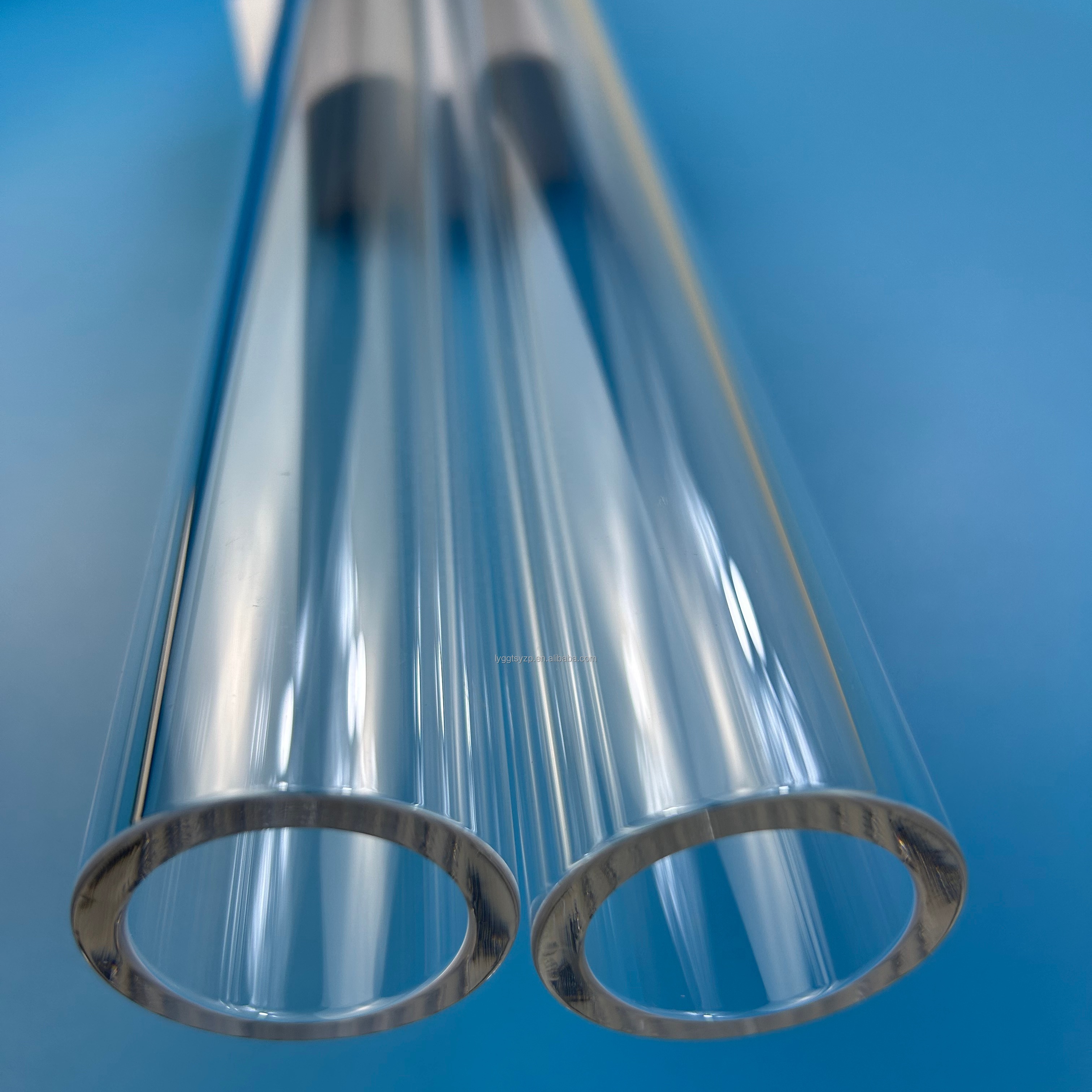
Semiconductor Furnace Heater Twin Tube
Rigid geometric wall tolerance, certified heavy metal bubble free inclusions, specialized for epitaxial growth and oxidation lines.
Product Details →Top 10 Quartz Optical Plate Suppliers Serving Kobe (2025 Evaluation)
A multi-dimensional audit cross-referencing surface planarity (λ/10 to λ/20), laser damage threshold (LDT), dimensional CNC tolerances (±0.005 mm), and Hanshin supply chain accessibility.
The manufacturing ecosystem of Kobe and the broader Kansai area—anchored by biomedical pioneers on Port Island (Kobe Biomedical Innovation Cluster - KBIC), optical component developers in Nishi-ku, and maritime robotics centers—demands exceptional purity and zero internal inclusions in fused silica components. When selecting a precision supplier, engineering teams evaluate raw crystalline provenance, hot flame annealing consistency, and CNC ultrasonic machining tolerances.
| Supplier Name | Primary Production Focus | Material Purity / Optical Grade | Machining Capabilities | Kobe Logistics Lead Time |
|---|---|---|---|---|
| Zunex Quartz Products Co., Ltd. | Custom Fused Quartz Plates, Wafers, Multi-bore Tubes | JGS1 (DUV), JGS2 (UV-VIS), JGS3 (IR) ≥99.99% | Laser micro-drilling, CNC ultrasonic milling, λ/10 double-side lap | 3-5 Days (Express Door-to-Door to Kobe/Osaka) |
| Tosoh Quartz Corporation | Semiconductor Quartzware, Photomask Substrates | Synthetic Fused Silica, Ultra-Low OH Content | Large-aperture CNC grinding, automated cleanroom fabrication | Local Domestic Stock / 2-4 Weeks Custom |
| Shin-Etsu Quartz Products Co., Ltd. | Synthetic Quartz Ingots, Optical Preforms | Extreme UV Lithography (EUV) Grade | High-purity chemical etching, ultra-flat double-sided polish | Domestic Kansai Distribution Hub |
| Nikon Corporation (Specialty Glass) | Synthetic Silica Optical Windows, Laser Elements | Deep-UV Grade Silica (Excimer-rated) | Wavefront interferometry-guided CNC corrective polishing | Production Lead Time: 4-6 Weeks |
| AGC Inc. (Fine Glass Division) | Optoelectronic Substrates, Synthetic Quartz | Synthetic Fused Silica with High LDT | Precision slicing, chamfering, thin-wafer chemical polishing | Domestic Hub / 1-2 Weeks Expedited |
| Heraeus Conamic Japan | Base Material Ingots, Diffusion Tubes, Plates | Suprasil, Infrasil, Homosil optical quartz | Large-format wafer slicing, flame restructuring | Regional Delivery: 1-3 Weeks |
| Sumita Optical Glass, Inc. | High-refraction lenses, Custom Optical Windows | Precision Functional Optical Glass & Quartz | Precision glass molding, CNC lens profiling | Domestic Dispatch: 2-3 Weeks |
| Ohara Inc. | Low-expansion ceramics, Substrate Plates | High transmission quartz-like ceramics | High-precision optical lapping (pitch polishing) | Domestic Kansai Route: 1-2 Weeks |
| Taiyo Nippon Sanso (Optics Division) | Gas-treated quartz reactors, Optical Cell Plates | High thermal stability fused quartz | Precision quartz pipe welding, burner flame annealing | Domestic Hub: 7-10 Days |
| Kanto Quartz Corporation | Semiconductor cleaning baths, Quartz trays | Standard Electronic & Solar Grade Silica | Bending, cutting, fire polishing, acid leaching | Domestic: 2-3 Weeks |
Technical Procurement Takeaway: While domestic Japanese manufacturers maintain strong localized stock for standardized wafer dimensions, Zunex Quartz delivers a distinctive advantage for R&D institutes and bespoke system developers in Kobe. By combining high-purity Donghai crystalline feedstocks with in-house laser micro-drilling, specialized grooving, and direct-to-engineer drawing evaluations (≤2 hour turnaround), custom non-standard orders bypass domestic 6-to-8-week retooling delays.
Localized Applications in Kobe & Kansai Industrial Clusters
Bridging synthetic fused silica performance with mission-critical applications across Hyogo's advanced manufacturing hubs.
KBIC Life Science & Flow Cytometry
The Kobe Biomedical Innovation Cluster relies on ultra-pure JGS1 quartz optical plates for laser-induced fluorescence (LIF) microfluidic chips. Zero bubble inclusion (DIN 3140-1) and high transmittance at 266nm–355nm ensure uncompromised single-cell detection fidelity.
Marine Robotics & High-Pressure Viewports
Supporting offshore robotics operating from Kobe Port. Double-side polished quartz plates exhibit 1100 MPa compressive strength, zero micro-fracturing along CNC bevels, and verified structural integrity in high-salinity marine submersibles.
GaN & SiC Epitaxy (Kansai Mega-Foundries)
With Wide Bandgap (WBG) power semiconductors ramping up in Osaka Bay and Harima, our quartz reaction tubes and wafer holders withstand sustained thermal profiles above 1150°C without recrystallization (devitrification) or metallic outgassing.
Emerging Technological Trends in Kansai's Quartz Ecosystem
Structural shifts transforming how Japanese optical engineers specify fused silica and quartz optical plates.
1. Migration Toward Cold Laser Machining (Pico/Femtosecond Ablation): Traditional ultrasonic grinding on fragile quartz plates often introduces subsurface micro-cracks measuring 10–30 μm deep. In Kobe's advanced photonics laboratories, femtosecond laser processing now provides damage-free edge rounding and micro-hole arrays with roughness Ra < 0.2 μm, eliminating brittle fracture points under high thermal cycling.
2. Low-Hydroxyl (<1 ppm OH) Synthetic Silica for Mid-IR Sensing: Driven by green hydrogen infrastructure projects along Kobe's Waterfront (such as liquefied hydrogen monitoring sensors), the demand for JGS3 infrared-grade optical quartz has surged. Standard silica exhibits a strong absorption dip around 2730nm due to OH vibration; specialized vacuum electric-fused quartz eliminates this band completely.
3. Extreme Homogeneity & Zero Striae for DUV Lithography: The miniaturization of precision optics requires refractive index homogeneity Δn across the substrate to stay within ±1×10⁻⁶. Rigorous thermal stress annealing guarantees stress birefringence below 2 nm/cm, crucial for high-numerical-aperture UV illumination systems.
Comparative Chemistry & Transmission Standards
Select your optical substrate with verified physical and chemical metrics.
| Parameter / Metric | JGS1 (Synthetic Fused Silica) | JGS2 (Optical Fused Quartz) | JGS3 (Infrared Fused Quartz) |
|---|---|---|---|
| Optical Transmittance Band | 185 nm – 2,500 nm (Deep UV) | 220 nm – 2,500 nm (UV-Visible) | 260 nm – 3,500 nm (Near-to-Mid IR) |
| Hydroxyl Content ([OH‾]) | Typical: 800 – 1200 ppm | Typical: 150 – 200 ppm | ≤ 2 ppm (Low OH Formulation) |
| Purity (SiO₂ wt %) | ≥ 99.999% | ≥ 99.99% | ≥ 99.99% |
| Refractive Index (nd @ 587.6 nm) | 1.4584 | 1.4585 | 1.4585 |
| Thermal Expansion (0–300 °C) | 5.5 × 10⁻⁷ K⁻¹ | 5.5 × 10⁻⁷ K⁻¹ | 5.5 × 10⁻⁷ K⁻¹ |
| Softening / Strain Point | 1600 °C / 1070 °C | 1683 °C / 1120 °C | 1720 °C / 1180 °C |
Frequently Asked Questions (Kobe Buyer Technical FAQ)
Key technical concerns addressed by our senior glass fabrication engineers.
How do you guarantee cleanroom-compatible cleanliness and defect-free surfaces for Kobe optical research labs?
What are the tariff codes, customs clearance routes, and shipping timelines for Kobe Port and Kansai Airport (KIX)?
Can Zunex provide custom stepped holes, beveled edges, and internal laser cavity grooving to STEP/DWG drawings?
What is the verification procedure for material grade authenticity between JGS1, JGS2, and JGS3?
Accelerate Your Precision Optical Development
Submit your DXF, DWG, PDF, or STEP files to our engineering group. Receive a comprehensive manufacturability assessment, tolerance verification, and competitive FOB/CIF Kobe pricing in 2 hours or less.
Contact Us