Engineered Quartz Glass Components for High-Spec Applications
Direct-from-factory optical substrates, thermal diffusion process tubes, and specialized reactor vessels manufactured to sub-micron geometric tolerances according to your CAD drawings.
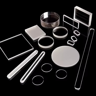
Custom Optical Quartz Test Sample Sheets
Ultra-flat fused transparent quartz substrates cut and polished for spectroscopic inspection, semiconductor cleanroom trials, and surface science evaluation.
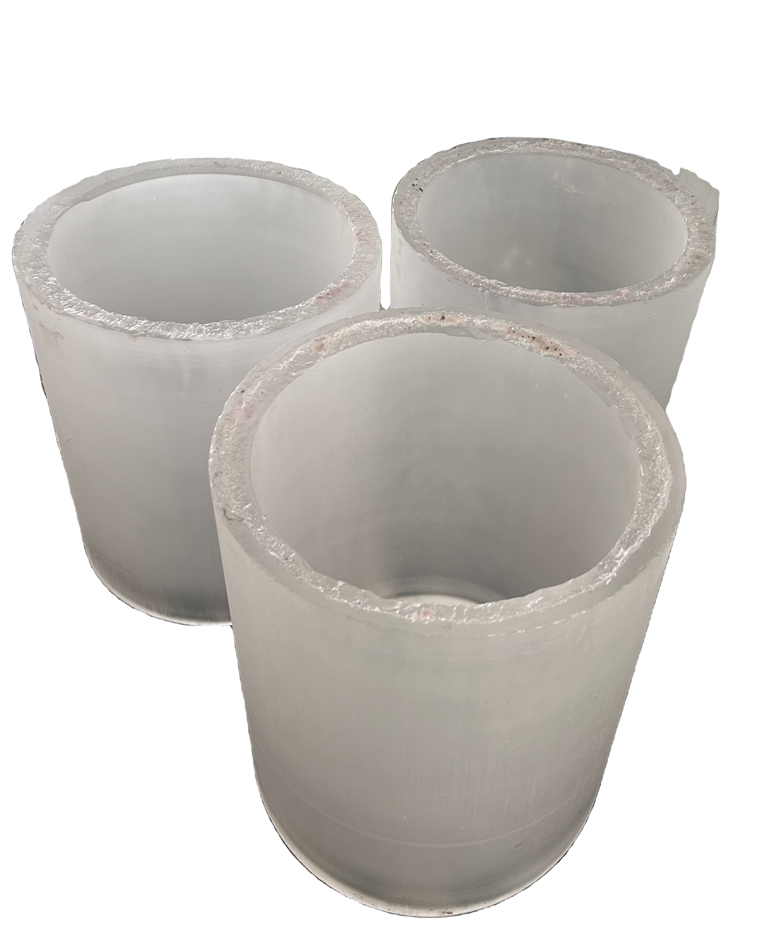
Open-Ended Frosted Quartz Cylinders & Ingots
Moulded, annealed, and flame-ground cylindrical fused silica stock ideal for diffuser tubes, furnace outer insulation, and optical fabrication blocks.
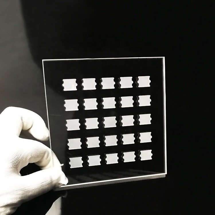
Optics Grade Fused Quartz Glass Plates
Available in thicknesses from 0.5mm to 100mm, offering superior deep-UV to near-IR transmission with double-sided optical diamond polishing.
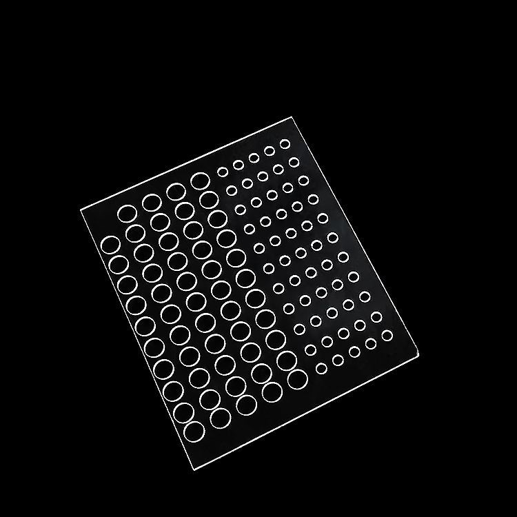
Zero-Background XRD Quartz Sample Holders
Precision micro-machined circular fused quartz disks eliminating stray diffractive scatter, critical for materials characterization in Kansai research labs.

High-Temperature Polished UV Quartz Discs
Continuous 1100°C thermal stability window disks engineered for ultraviolet curing viewports, plasma observation, and photolithography stages.
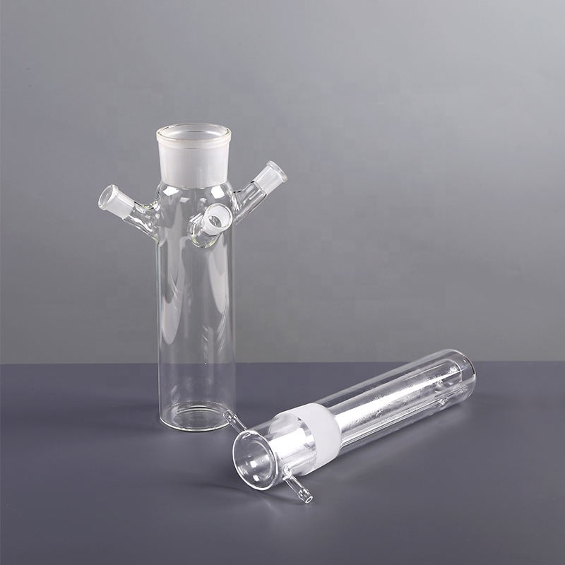
Photocatalytic Quartz Reactors & Vessels
Custom internal illumination reaction chambers with multi-port gas inlets, torch-welded flanges, and high UV transmittance for clean energy trials.
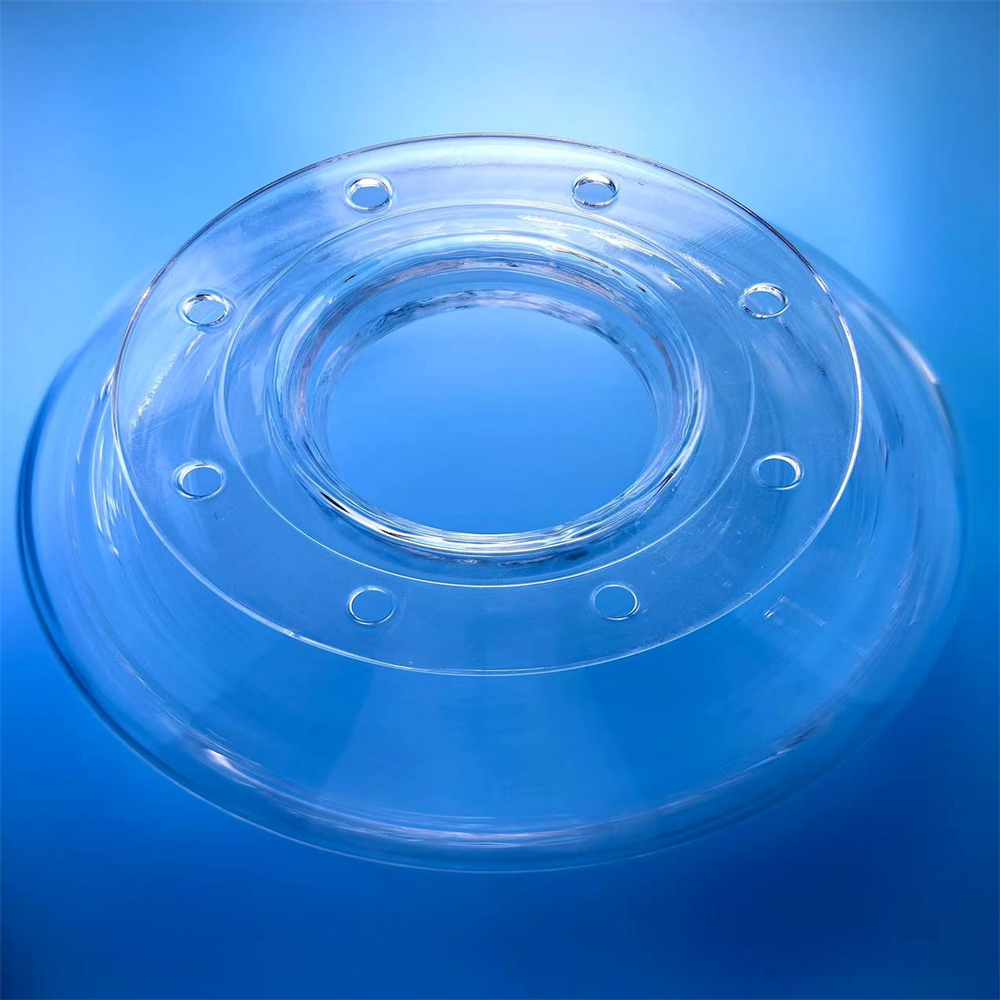
Twin-Tube Emitters & Flanged Process Tubes
High-rigidity twin-bore quartz bodies and custom KF/ISO ground quartz flanges engineered for infrared rapid thermal processing and CVD diffusion chambers.
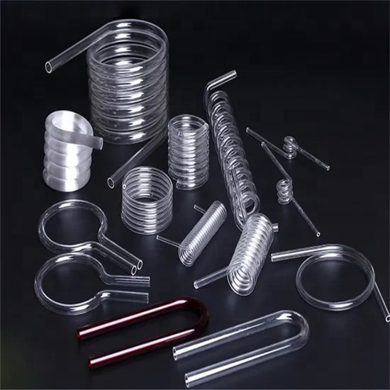
U-Bent & Spiral Fused Quartz Manifolds
Complex bent geometry tubes, spiral condensation coils, and custom heating elements bent with robotic precision without internal cross-sectional thinning.
The Strategic Importance of High-Purity Quartz Glass in Kyoto's Industrial Corridor
Kyoto Prefecture, while historically celebrated as the cultural capital of Japan, represents one of East Asia’s most dense and sophisticated epicenters of precision engineering, semiconductor capital equipment, advanced ceramics, and analytical instrumentation. From global headquarters and cleanrooms in Minami-ku and Ukyo-ku to the pioneering laboratories of Kansai Science City (Keihanna) and Kyoto University's Katsura Campus, the regional requirement for high-specification vitreous silica is among the most demanding in the international marketplace.
Industrial quartz glass—specifically high-purity fused silica (synthetic SiO₂) and natural fused quartz—serves as the foundational, non-negotiable substrate across Kyoto's production lines. Whether facilitating plasma etch containment in sub-5nm semiconductor fabrication, providing absolute spectral transparency in atomic absorption spectrometers, or serving as chemically inert reaction chambers in green nanotechnology synthesis, quartz glass provides an unmatched balance of thermal, chemical, and optical attributes.
Physical and Thermomechanical Superiority of Fused Quartz
Unlike standard borosilicate or aluminosilicate glasses, vitreous silica contains almost exclusively silicon dioxide (SiO₂ ≥ 99.99%), possessing a disordered, non-crystalline three-dimensional polymer network bonded entirely by strong Si-O tetrahedral links. This unique amorphous atomic configuration yields several critical engineering properties:
Thermal Shock Resistance
Features an extraordinarily low thermal expansion coefficient of 5.5 × 10⁻⁷ /°C (from 20°C to 320°C). Quartz glass tubes can withstand violent temperature fluctuations—such as being pulled from a 1100°C diffusion furnace and immediately plunged into cold water without structural cleavage or mechanical micro-fracturing.
Broadband Optical Transmission
Optical-grade synthetic fused silica (JGS1) exhibits exceptional transmission (>90%) spanning from the Deep Ultraviolet (DUV 185 nm) through the visible light spectrum to near-infrared (NIR 2500 nm), completely free of internal inclusions, striae, and metallic absorption bands.
Extreme Chemical Inertness
Impermeable and inert to almost all acidic reagents, halogens, and aggressive cleaning compounds—including boiling nitric, sulfuric, and hydrochloric acids. Only hydrofluoric acid (HF) and concentrated phosphoric acid at elevated temperatures (>150°C) attack its protective silicon network.
Standard Material Specification Matrix for Kyoto Engineering Teams
Engineers purchasing quartz components in Kansai must calibrate the correct optical grade against operating temperatures, hydroxyl (OH⁻) content, and allowable trace metal budgets (e.g., Fe, Al, Cu, Na). Below is the comparative baseline used by Zunex Quartz when consulting on Japanese OEM drawings:
| Material Classification | Optical Transmission Band | Typical OH⁻ Content | Softening / Working Point | Primary Industrial Sector |
|---|---|---|---|---|
| JGS1 (Synthetic Silica) | 185 nm – 2,500 nm (Deep UV) | < 5 ppm – 1,200 ppm (Grade specific) | 1683°C / 1150°C | Excimer lasers, photolithography, UV viewports |
| JGS2 (Optical Quartz) | 220 nm – 2,500 nm (Standard UV-Vis) | < 30 ppm | 1670°C / 1100°C | Optical sight glasses, analytical cell bodies |
| JGS3 (Infrared Silica) | 260 nm – 3,500 nm (Low OH⁻) | < 2 ppm – 5 ppm | 1680°C / 1120°C | Infrared heating emitters, pyrometry tubes |
| High-Purity Clear Quartz (Tubing) | 260 nm – 2,800 nm | < 20 ppm | 1683°C / 1150°C | Semiconductor diffusion, LPCVD, furnace liners |
Localized Application Scenarios: Serving Kyoto's Advanced Tech Clusters
To supply quartz components reliably to Kyoto businesses, a manufacturer must understand the localized engineering nuances across the region’s premier technological hubs.
Semiconductor & Power Devices
Kyoto is the global cradle for wide-bandgap semiconductors (Silicon Carbide - SiC, Gallium Nitride - GaN). High-purity quartz furnace tubes, wafer handling boats, and gas injection nozzles ensure zero heavy-metal ion contamination during epitaxial growth and high-temperature dopant annealing (>1050°C).
Analytical & Medical Optics
Kyoto’s analytical giants require micro-cuvettes, flow cells, and spectrometry windows polished to a surface roughness of Ra < 0.2 nm. Eliminating wavefront distortion is mandatory for high-resolution liquid chromatography (HPLC) UV detectors and atomic absorption sensors.
Photocatalysis & Green Energy
University labs and clean-tech startups across Keihanna rely on our customized double-jacketed quartz reactors. Exceptional UV penetration allows artificial sunlight and 254nm irradiation to degrade volatile organic compounds (VOCs) and power experimental water-splitting hydrogen systems.
Advanced Nanomaterials & XRD
In materials synthesis facilities throughout Kansai, our zero-background circular fused quartz XRD sample holders isolate diffractometer background noise, giving crystallographers unobstructed resolution when analyzing non-crystalline powders and thin films.
Regional Procurement Trends in Kyoto & the Kansai High-Tech Corridor
Procurement practices across Japanese technology companies have evolved dramatically. B2B procurement managers and fab maintenance engineers in Kyoto are moving away from multi-layered domestic trading monopolies ("Shosha") toward agile, direct-from-manufacturer partnerships that offer verified quality control and transparent manufacturing pricing. Several notable trends characterize the current landscape:
1. Direct CAD-to-Flame Customization
Standard off-the-shelf catalog tubes no longer meet the stringent tolerances of modular CVD and atomic layer deposition (ALD) chambers. Kyoto equipment manufacturers routinely require specialized flange welds, laser micro-slotted injector holes, and custom U-bends. Direct communication with quartz fabrication factories capable of reading 3D STEP and DWG files eliminates costly translation errors and reduces prototyping cycles by up to 60%.
2. Stringent Trace Contamination Control
With Kyoto's semiconductor sector spearheading power conversion modules for electric vehicles (EVs) and high-speed rail, metal-ion tolerance budgets have tightened. Contaminants such as Copper (Cu), Iron (Fe), and Sodium (Na) within quartz tubes can migrate into silicon substrates during diffusion cycles, degrading gate dielectric integrity. Manufacturers must supply batch-level Inductively Coupled Plasma Mass Spectrometry (ICP-MS) purity documentation.
3. Supply Chain Redundancy and Rapid Lead Times
Post-pandemic procurement protocols emphasize supply chain diversification. Relying solely on local Japanese torch shops has proven bottleneck-prone due to domestic labor constraints. Forward-thinking Kyoto procurement directors maintain dual-sourcing architectures, combining local stock with scalable industrial manufacturers based in China's quartz capital (Donghai), ensuring uninterrupted access to raw ingots and fast-turnaround quartz machining.
Zunex Quartz: Direct Factory Engineering Advantage for Kyoto Buyers
Headquartered in Donghai County, Jiangsu—the premier raw silica processing hub—Zunex Quartz Products Co., Ltd. delivers high-precision fused quartz glass solutions directly to engineering teams across Japan and worldwide. We integrate upstream high-purity ingot smelting with advanced downstream precision finishing, delivering distinct competitive advantages:
Precision CNC & Laser Finishing
Equipped with state-of-the-art quartz laser cutting, precision hole drilling, micro-grooving, and ultrasonic 5-axis CNC equipment. We execute tight dimensional tolerances of ±0.05 mm on custom optical plates, flange grooves, and wafer carriers without thermal micro-cracking.
Verified Rapid Technical Review
Every RFQ submitted by Kyoto engineering teams receives an immediate review by our senior quartz materials engineers. We guarantee an average technical response time of ≤ 2 hours, confirming manufacturability, thermal annealing curves, and freight estimates before quote delivery.
Export Protection & Direct Air Logistics
Fragile quartz tubing and optical sheets are packed using shock-absorbing foam molds, vacuum shrink-wrapping, and heavy-duty ISPM-15 export wooden crates. Direct daily air express cargo from Shanghai/Lianyungang to Kansai International Airport (KIX) ensures 3-to-5 day door-to-door delivery in Kyoto.
Frequently Asked Questions: Kyoto B2B Quartz Glass Procurement
Key technical, quality, and commercial inquiries addressed by our international trade and engineering departments when fulfilling orders for Japanese clients.
Yes. We regularly fabricate components complying with Japanese Industrial Standards (JIS B 0405 for general tolerances and JIS R 3201 for glass processing). Our engineering department natively accepts 2D/3D CAD formats including DWG, DXF, STEP, IGES, and dimensioned PDF technical drawings with standard Japanese tolerance annotations.
Our flanged quartz tubes are fabricated using specialized automatic thermal lathe welding followed by precision optical diamond face lapping. Flange surfaces achieve high flatness (≤ 2 light bands) to guarantee hermetic helium leak rates below 1 × 10⁻⁹ mbar·l/s when paired with fluoroelastomer O-rings (Viton) or metal CF seals in high-vacuum chambers.
Standard prototypes (such as custom-sized optical windows or laser-cut XRD holders) typically require 5 to 8 working days in production. Complex flame-welded reactors or twin-tube configurations take approximately 10 to 14 working days. Air express shipments clear Kansai Customs (KIX) and arrive in Kyoto cleanrooms within 3 to 4 days.
Clear fused quartz maintains structural integrity continuously up to 1100°C and short-term up to 1300°C. However, sustained exposure above 1150°C in the presence of surface alkali contaminants can induce devitrification (surface conversion to cristobalite). To maximize lifespan, all Zunex process tubes undergo thorough cleanroom de-hydroxylation and acid-wash etching before shipment.
Long tubes and cylinders are individually cushioned inside custom-molded high-density polyethylene (EPE) foam sleeves, suspended inside reinforced multi-ply corrugated inner boxes, and secured within palletized solid-wood export crates. Our verified transit damage rate on international air shipments remains below 0.2%.
Yes. We actively support university laboratories, R&D spin-offs, and pilot production lines across Kyoto University, Doshisha, and Keihanna science parks. We maintain zero minimum order quantity (MOQ) restrictions for custom research prototypes, providing comprehensive quotation sheets within two hours.
Accelerate Your Quartz Component Procurement
Submit your CAD blueprints, technical sketches, or material specifications today. Our engineering staff provides immediate manufacturability feedback, material grade selection assistance, and rapid factory pricing tailored for Kyoto's high-tech manufacturing sector.